
Optical-Grade JGS2 Wafers for Research
JGS2 fused silica is an option for transparent optical substrates and insulating support wafers. Researchers select the grade by optical transmission, surface quality, process temperature, and dimensional requirements.
Discuss custom diameters, thicknesses, polishing options, scratch-dig limits, and optical tolerances with UniversityWafer. Availability and pricing depend on the final specification and quantity.
Common Substrate Applications
- Optical windows and instrument viewports
- Substrates for coated mirrors, lenses, and other optical components
- Transparent supports for thin-film deposition
- MEMS structures and sensor research
- Optical and photonic device experiments
- Carrier or support substrates in semiconductor process development
Request a JGS2 Fused Silica Quote
Send your wafer diameter or sample dimensions, thickness and tolerance, single-side or double-side polish, operating wavelength, quantity, and required delivery date.
Get Your Quote Fast! Or Buy Fused Silica Wafers Online and start researching today.
JGS2 Fused Silica Transmission Curve
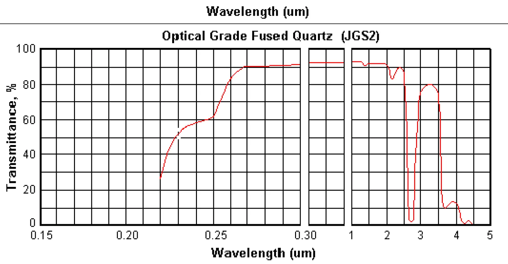
Use this curve as a material-selection reference. Request transmission data for your exact wavelength and substrate thickness before finalizing an optical design.
MEMS Research Example: Two-Inch Fused Quartz Wafers
A university researcher requested two-inch fused quartz wafers, 1 mm thick, in both single-side-polished and double-side-polished versions for MEMS fabrication.
This example illustrates a substrate inquiry; confirm the required grade and polish for your own process. Reference #226827 for specifications and pricing.
What Is JGS2 Fused Silica?
JGS2 fused silica, also called JGS2 fused quartz or optical quartz glass, is an amorphous silicon dioxide material. It is distinct from single-crystal quartz, which has a crystalline structure and direction-dependent properties.
JGS2 is commonly considered for visible and near-infrared optical windows, laboratory substrates, and support wafers. For demanding ultraviolet work, compare its short-wavelength performance with JGS1 UV-grade fused silica. A grade name alone does not establish transmission at every wavelength.
JGS2 Optical Properties and Transmission
Optical performance depends on substrate thickness, surface polish, inclusions, impurities, coatings, and hydroxyl (OH) content. Specify your operating wavelength and minimum acceptable transmission when ordering a JGS2 window.
The reference data below lists a transmission interval of 0.26–2.10 µm (260–2100 nm) with average transmission above 85%. These figures require test conditions, sample thickness, and supplier confirmation to be useful as acceptance criteria. They should not be interpreted as a uniform transmission guarantee throughout the interval.
OH-related absorption can limit infrared performance, including around 2.7 µm. For infrared-focused projects, compare JGS3 fused silica and obtain wavelength-specific data. For optical modeling, also review the refractive index at the design wavelength.
JGS2 Reference Material Characteristics
The following values are retained from the page's material reference. They are not lot-specific measurements. Confirm dimensions, optical quality, and material properties on the quotation or supplier datasheet.
| JGS2 Fused Silica Parameter | Reference Value |
| Maximum Size | <300mm |
| Transmission Range | 0.26–2.10µm |
| Average Transmission | >85% |
| OH Content | 150ppm |
| Impurity Content | 20–40ppm |
| Stress Birefringence | 4–6 nm/cm |
| Melting Method | Oxy-hydrogen melting |
A listed maximum material size does not establish availability of every wafer diameter, thickness, or polish combination. Request current fabrication options for your dimensions.
JGS2 Substrates for MEMS and Semiconductor Processing
Fused silica can provide an electrically insulating, transparent platform for MEMS and sensor research. Select substrate thickness and flatness for handling, alignment, and the subsequent fabrication steps. Its low thermal expansion is useful when dimensional changes would affect a device or optical assembly.
For processes involving photolithography, specify surface quality and flatness along with compatibility with your exposure and alignment setup. For atomic layer deposition (ALD) or other coating processes, define surface preparation, film chemistry, and thermal limits. JGS2 is a substrate; it does not replace the active semiconductor layer in an electronic device.
Single-Side vs. Double-Side Polished JGS2 Wafers
Single-side polish (SSP) may suit work focused on one prepared surface. Double-side polish (DSP) is often requested when light passes through both surfaces or when both sides require processing. Specify surface roughness, parallelism, flatness, and scratch-dig limits separately; a polish designation alone does not define all optical tolerances.
JGS1 vs. JGS2 vs. JGS3: Which Grade Fits?
- JGS1: Commonly considered for deep-UV and visible optics where purity and short-wavelength transmission are priorities.
- JGS2: An optical-grade option for visible and near-infrared windows, laboratory substrates, and MEMS support wafers, subject to the specified optical quality.
- JGS3: Often evaluated for infrared applications requiring reduced OH absorption.
Use the JGS1 and JGS2 material-property comparison and supplier transmission curves to select a grade. Manufacturer trade names are not automatic equivalents: compare homogeneity, OH content, inclusions, and finished-part tolerances.
How to Specify a Custom JGS2 Optical Substrate
- Geometry: Diameter or length × width, thickness, tolerances, and edge finish.
- Optical use: Operating wavelength, required transmission, clear aperture, and whether light passes through the substrate.
- Surface quality: SSP or DSP, surface roughness, scratch-dig limits, flatness, and parallelism.
- Process conditions: Coatings, cleaning requirements, temperature cycle, and chemical exposure.
- Delivery: Quantity, packaging, requested documentation, and delivery date.
For laser windows, add pulse duration or continuous-wave operation, incident power or fluence, and coating requirements. Laser-damage performance must be established for the finished optic and operating conditions.
Questions About JGS2 Fused Silica Wafers
Is JGS2 the same as crystalline quartz?
No. JGS2 is an amorphous glass. Specify single-crystal quartz if the design requires a crystal cut or direction-dependent optical or piezoelectric properties.
Can JGS2 be used for UV transmission?
It depends on the wavelength, material quality, and optical path length. For demanding UV applications, request measured transmission and compare JGS1 before selecting a substrate.
Can I order custom thicknesses or small quantities?
Send the dimensions, tolerance, polish, and quantity for an availability check. The MEMS inquiry on this page provides one example of custom wafer specifications.