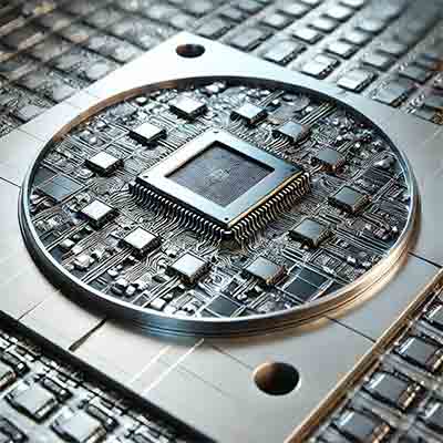
Silicon Germanium Used to Fabricate Microchips
A microchip engineer requested a qutoe for the following.
I am interested in purchasing Synthetic Germanium Wafers (SiGe) Wafers. They use them as semiconductors in microchips. I have listed the specs below.
Diameter 4.7"
Thicknesses: 2mm (+/- 0.005mm)
Tolerance: (+/- 0.005mm)
Dopants: Ge/Germanium
Thermal Oxidation: wet or dry - thickness range 25nm to > 4µm
Heat Tolerance: + 125 C
Composition: GE = 12-17%
Reference #133489 for specs and pricing.
Get Your FAST! Or, Buy Online and Start Researching Today!
What Substrates are Used to Fabricate Microchips?
We use these in a PDMS spinner to apply this coats of PDMS. We do not intend to use them for microchip
fabrication.
The most common substrates used to fabricate microchips are silicon wafers. Below are the key specifications typically associated with these substrates:
1. Silicon Wafers
- Material: High-purity monocrystalline silicon

- Diameter: Commonly 150 mm (6 inch), 200 mm (8 inch), and 300 mm (12 inch)
- Thickness: Varies with diameter; typically 675 µm for 200 mm wafers and 775 µm for 300 mm wafers
- Crystal Ori: (100) or (111) planes are most common
- Doping Type: p-type (boron) or n-type (phosphorus or arsenic)
- Resistivity: Ranges from 1 to 20 Ω·cm depending on the application
- Surface Finish: Polished on one side (prime wafer) or both sides (double-sided polished)
- Flatness: Highly controlled with a total thickness variation (TTV) typically less than 2 µm
- Edge Profile: Rounded edges to prevent chipping and damage during handling
2. SOI (Silicon on Insulator) Wafers
- Structure: Thin silicon layer separated from the bulk silicon substrate by an insulating layer (usually silicon dioxide)
- Top Silicon Layer Thickness: Ranges from 10 nm to several micrometers
- Buried Oxide Layer Thickness: Typically 100 nm to 3 µm
- Wafer Diameter: Similar to standard silicon wafers (150 mm, 200 mm, 300 mm)
- Surface Finish: Polished top layer for device fabrication
3. Compound Semiconductor Substrates
- Material: Gallium arsenide (GaAs), Silicon carbide (SiC), Sapphire (Al2O3)
- Applications: High-frequency, optoelectronic, and high-power devices
- Specifications:
- GaAs: Typically 4-inch (100 mm) diameter, semi-insulating with a resistivity greater than 10⁷ Ω·cm
- SiC: Diameter ranges from 100 mm to 200 mm, available in 4H or 6H polytypes
- Sapphire: Diameters usually 100 mm or 150 mm, with high optical transparency and thermal conductivity
These substrates are selected based on the specific requirements of the microchip being fabricated, including electrical, thermal, and mechanical properties. Silicon remains the dominant substrate due to its well-established processing technology and cost-effectiveness.

