
I have a quick question about solar wafers versus silicon wafers. When a solar wafer is designated as n-type or p-type, does being a solar wafer imply that a p-n junction has already been grown, or is it simply bulk p-type or n-type silicon? I am looking to start with a small quantity of approximately 25 wafers.
Silicon Wafers for P-N Junction Research
P-N junction research begins with carefully controlled semiconductor materials. UniversityWafer supplies silicon wafers with different conductivity types, dopants, resistivities, crystal orientations, thicknesses, and surface finishes for semiconductor device fabrication and research.
A p-n junction is created when a p-type semiconductor region and an n-type semiconductor region are brought into contact within a semiconductor structure. In silicon, these regions are typically produced by introducing controlled concentrations of acceptor or donor dopants.
Researchers can begin with a uniformly doped wafer and form the opposite conductivity type near the surface through processes such as diffusion or ion implantation. Alternatively, wafers containing pre-fabricated junction structures may be used when available.
Does an N-Type or P-Type Wafer Already Have a P-N Junction?
No—not necessarily. A wafer described simply as p-type silicon or n-type silicon normally refers to the conductivity type of the bulk silicon.
A uniformly doped p-type wafer does not automatically contain an n-type region, and a uniformly doped n-type wafer does not automatically contain a p-type region. Therefore, the conductivity designation by itself does not indicate that a p-n junction has already been fabricated.
This distinction is especially important when purchasing wafers described as solar wafers. The term may describe silicon intended for photovoltaic research or manufacturing, but researchers should verify whether the material is simply a doped silicon substrate or whether a junction/emitter structure has already been formed.
Researcher Question: Solar Wafer vs. Silicon Wafer
The answer depends on the specific wafer specification. A p-type solar silicon wafer may simply be a p-type substrate. To obtain an n-on-p junction, for example, an n-type surface region can be formed in the p-type substrate using a donor such as phosphorus.
Researchers looking for a pre-formed junction should therefore specify the desired junction configuration, substrate conductivity type, dopant, resistivity, junction depth or doped-layer thickness, carrier concentration, wafer diameter, orientation, and surface finish.
Example N-on-P Silicon Junction Wafer
The following is an example of a silicon wafer specification previously quoted for p-n junction and photovoltaic research:
| Specification | Example Value |
|---|---|
| Item | GX82j |
| Wafer Diameter | 4 inch |
| Thickness | 300 ± 25 µm |
| Base Material | p-type Si:B |
| Orientation | (100) ± 0.5° |
| Base Resistivity | 5–10 Ω·cm |
| Surface Finish | Double-side polished (DSP) |
| N-Type Surface Region | Phosphorus-diffused layer |
| Approx. Diffused-Layer Depth | ~1 µm |
In this example, the boron-doped p-type silicon forms the base, while phosphorus introduces an n-type region near the surface. The interface between these differently doped regions forms the p-n junction.
Reference #265226 for pricing.
How a Silicon P-N Junction Forms
When p-type and n-type silicon regions meet, electrons initially diffuse from the n-type side toward the p-type side, while holes diffuse in the opposite direction. Electrons and holes recombine near the interface.
This process leaves behind ionized dopant atoms that are fixed in the crystal lattice. The resulting region has a greatly reduced concentration of mobile carriers and is called the depletion region or space-charge region.
These fixed charges establish a built-in electric field and electrostatic potential barrier. At thermal equilibrium, the electric-field-driven carrier transport balances diffusion so that there is no net current through an isolated junction.
Forward Bias and Reverse Bias
Forward Bias
A p-n junction is forward biased when the p-type side is connected to a higher electrical potential than the n-type side. The applied voltage reduces the junction's potential barrier and narrows the depletion region, allowing substantially increased carrier injection across the junction.
Reverse Bias
A junction is reverse biased when the p-type side is connected to a lower electrical potential than the n-type side. This increases the potential barrier and generally widens the depletion region.
Only a relatively small reverse current normally flows before breakdown, although the exact behavior depends on semiconductor material, doping concentration, junction geometry, defects, temperature, and applied voltage.
Choosing Silicon Wafers for P-N Junction Fabrication
The correct starting substrate depends on how the junction will be fabricated and characterized. Important wafer specifications include:
- Conductivity type – choose p-type or n-type starting silicon according to the intended device structure.
- Dopant – common silicon dopants include boron for p-type material and phosphorus or arsenic for n-type material.
- Resistivity – relates to dopant concentration and carrier mobility and is an important parameter in device design.
- Crystal orientation – (100), (110), and (111) silicon have different crystallographic properties that can affect fabrication processes.
- Growth method – float-zone (FZ) and Czochralski-grown silicon offer different impurity and oxygen characteristics.
- Surface finish – single-side polished (SSP) or double-side polished (DSP) material may be selected according to the process.
- Wafer thickness and diameter – should be compatible with fabrication, handling, and processing equipment.
- Minority-carrier lifetime – can be particularly important for photovoltaic, detector, and other carrier-lifetime-sensitive experiments.
Silicon Wafers for Photovoltaic P-N Junction Research
P-n junctions are fundamental to conventional crystalline-silicon photovoltaic cells. When photons with sufficient energy are absorbed, they can generate electron-hole pairs. Carrier-selective junction regions and the device's internal electrostatic structure help separate photogenerated carriers so they can be collected at electrical contacts.
Researchers studying photovoltaic devices may require tightly controlled substrate resistivity, carrier lifetime, surface condition, dopant concentration, and junction properties. These parameters can strongly influence recombination, carrier collection, and overall device performance.
P-N Junction Wafer Research Request
We are looking for n-on-p type Si and GaAs wafers. The wafer size is flexible, and we only need a small quantity of fewer than five wafers.
For a request like this, it is useful to specify whether a pre-formed junction is required or whether uniformly doped substrates will be used to fabricate the junction during the research process.
Additional specifications can include base conductivity type, target resistivity, junction depth, surface dopant concentration, crystal orientation, wafer thickness, polishing, diameter, and quantity.
Example Silicon Research Wafers
| Item | Material | Orientation | Diameter | Thickness | Polish | Resistivity |
|---|---|---|---|---|---|---|
| D063 | n-type Si:P | (100) ±1° | 4" | 280 µm | DSP | FZ, 1–5 Ω·cm |
| SEMI Prime PV FZ reference wafer, dual flats, TTV <6 µm, bow <5 µm, specified minority-carrier lifetime >13,934 µs. | ||||||
| K660 | n-type Si:P | (100) ±1° | 4" | 280 µm | DSP | FZ, 1–5 Ω·cm |
| SEMI Prime PV reference wafer, dual flats, specified minority-carrier lifetime >2,000 µs. | ||||||
Important: These examples are n-type starting wafers and should not be interpreted as containing a p-n junction unless the individual product specification explicitly states that an opposite-conductivity region has already been formed.
Can P-N Junction Wafers Be Diced?
Silicon wafers can be diced into smaller pieces when researchers need dies or substrate coupons instead of complete wafers.
When requesting dicing, specify the required die dimensions, quantity, kerf or dimensional tolerances, surface-protection requirements, and any restrictions on the usable wafer area. If a wafer already contains a junction or fabricated device structure, the location of those structures should also be considered when developing the dicing plan.
Common P-N Junction Applications
P-n junctions are fundamental building blocks in semiconductor technology and are used directly or as part of more complex device structures in:
- Rectifier and signal diodes
- Photodiodes and optical detectors
- Solar cells
- Light-emitting diodes (LEDs)
- Bipolar junction transistors
- Junction-based sensors
- Power semiconductor devices
- Integrated semiconductor structures
Request Silicon Wafers for P-N Junction Research
UniversityWafer supplies silicon substrates for semiconductor physics, diode fabrication, photovoltaic research, sensors, microelectronics, and university laboratories.
Get Your P-N Junction Wafer Quote FAST! Include your required conductivity type, dopant, resistivity, orientation, diameter, thickness, polish, quantity, and whether you require a pre-formed junction.
Or Buy Silicon Wafers Online and start researching today.
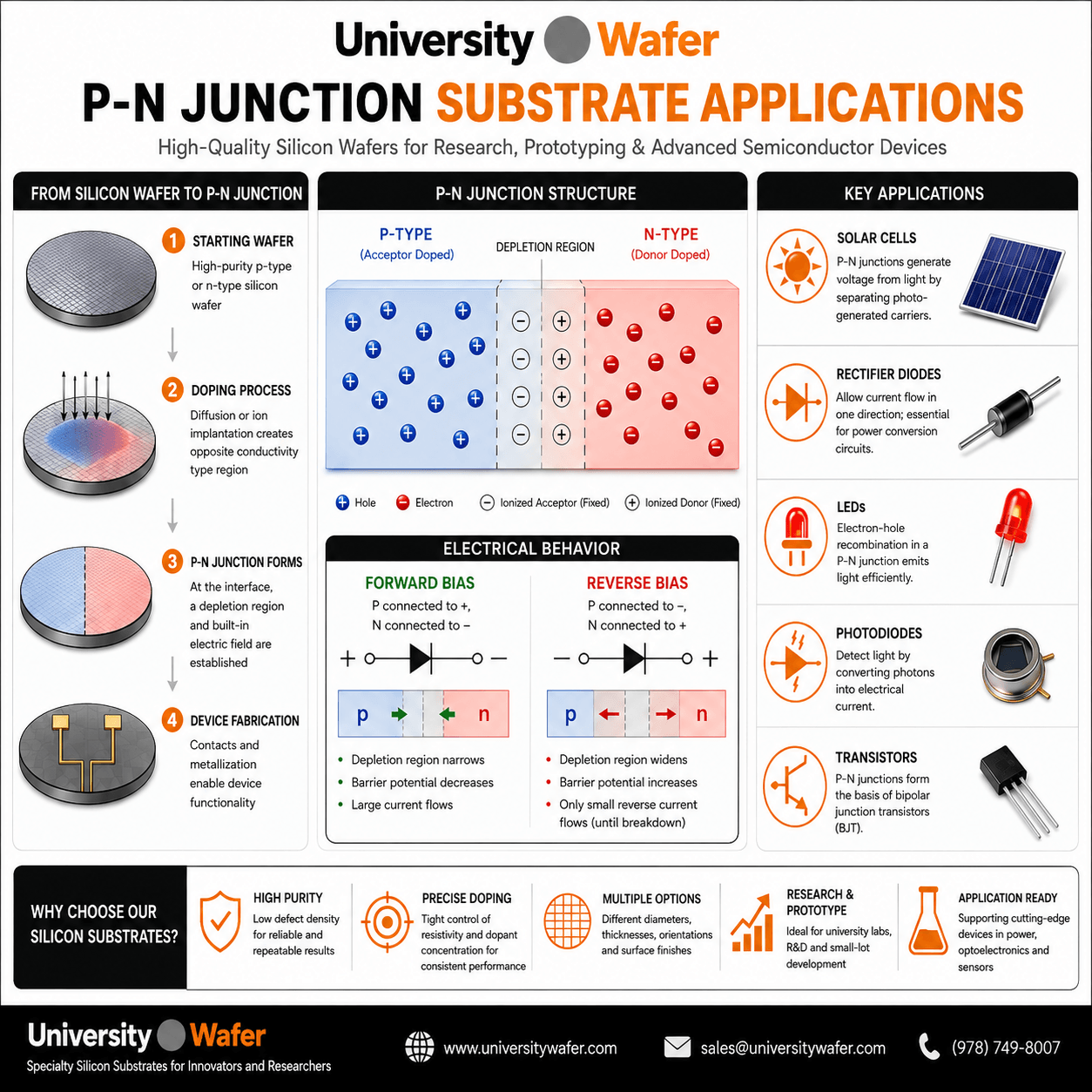
What Is a P-N Junction?
A p-n junction is the interface between p-type semiconductor and n-type semiconductor regions within a semiconductor structure. In silicon, these regions are created by controlled doping that changes the concentrations of electrons and holes available for electrical conduction.
In n-type silicon, electrons are the majority carriers and holes are the minority carriers. In p-type silicon, holes are the majority carriers and electrons are the minority carriers. Importantly, both bulk regions remain approximately electrically neutral; the terms "p-type" and "n-type" describe their dominant mobile charge carriers, not a net positive or negative electrical charge.
When these two regions form a junction, carrier diffusion produces a depletion region and a built-in electric field. This behavior gives the p-n junction its rectifying properties and makes it one of the fundamental structures used throughout semiconductor electronics.
How Does a P-N Junction Form?
Before the junction reaches equilibrium, the n-type region contains a relatively high concentration of mobile electrons while the p-type region contains a relatively high concentration of mobile holes. Because of these concentration gradients, electrons diffuse from the n-type side toward the p-type side and holes diffuse in the opposite direction.
Near the interface, electrons and holes recombine. Their movement leaves behind ionized donor atoms on the n-type side and ionized acceptor atoms on the p-type side. These dopant ions are fixed within the semiconductor crystal and cannot move freely through the material.
The resulting region has a much lower concentration of mobile carriers than the surrounding semiconductor and is called the depletion region or space-charge region.
The Built-In Electric Field and Potential Barrier
The fixed positive donor ions on the n-side and negative acceptor ions on the p-side create an internal electric field across the depletion region. This field opposes continued majority-carrier diffusion.
At thermal equilibrium, the carrier motion caused by this electric field balances diffusion, producing no net current through an isolated junction. The associated electrostatic potential difference is commonly described as the built-in potential.
The magnitude of the built-in potential and the width of the depletion region depend on factors including semiconductor material, temperature, and the acceptor and donor concentrations on each side of the junction.
Forward Bias vs. Reverse Bias
| Condition | Forward Bias | Reverse Bias |
|---|---|---|
| P-Type Connection | Higher potential (+) | Lower potential (−) |
| N-Type Connection | Lower potential (−) | Higher potential (+) |
| Depletion Region | Generally becomes narrower | Generally becomes wider |
| Potential Barrier | Reduced | Increased |
| Current | Increases strongly with sufficient forward bias | Small reverse current before breakdown |
What Happens During Forward Bias?
In forward bias, the p-type side is connected to a higher electrical potential than the n-type side. The applied voltage opposes the junction's built-in potential, reducing the effective barrier to carrier injection.
Electrons can then be injected from the n-type region into the p-type region, while holes are injected from the p-type region into the n-type region. These injected carriers become minority carriers after crossing the junction and contribute to the diode's forward current.
For an ordinary silicon diode, current does not suddenly begin at one universal "turn-on voltage." Instead, forward current varies approximately exponentially with junction voltage over an important operating range. Values around 0.6–0.7 V are often used as convenient approximations for the forward voltage of many silicon diodes at practical current levels, but the actual value depends on current density, temperature, device construction, and other parameters.
What Happens During Reverse Bias?
In reverse bias, the p-type region is held at a lower potential than the n-type region. The external voltage reinforces the junction's built-in field and generally increases the width of the depletion region.
Majority carriers are pulled away from the junction, so only a relatively small reverse current normally flows before breakdown. This current is influenced by minority-carrier generation, defects, temperature, junction area, and device design.
If the reverse voltage becomes sufficiently large, the junction can enter breakdown. Depending on doping and device structure, breakdown can involve Zener tunneling, avalanche multiplication, or a combination of the two.
P-N Junction Energy Bands
The p-n junction can also be understood using semiconductor energy-band theory . Before equilibrium, differently doped regions have different carrier concentrations and Fermi-level positions relative to their band edges.
When a p-n junction reaches thermal equilibrium, the Fermi level becomes spatially constant through the equilibrium structure. The conduction and valence band edges bend across the depletion region in response to the built-in electrostatic potential.
Applying forward or reverse bias changes the electrostatic potential and carrier distributions. Under nonequilibrium conditions, electron and hole populations can often be described using separate quasi-Fermi levels.
How Are Silicon P-N Junctions Fabricated?
Semiconductor manufacturers generally do not fabricate a silicon p-n junction by physically attaching separate pieces of p-type and n-type silicon. Instead, differently doped regions are created within a semiconductor wafer.
Common fabrication approaches include:
- Thermal diffusion – dopant atoms are introduced and redistributed through the silicon at elevated temperature.
- Ion implantation – accelerated dopant ions are introduced into selected regions of the wafer, followed by thermal processing to repair lattice damage and electrically activate dopants.
- Epitaxial growth – a crystalline semiconductor layer with controlled composition and doping can be grown on a crystalline substrate.
- In-situ doping – dopant species can be incorporated during certain semiconductor deposition or epitaxial growth processes.
Boron is widely used as an acceptor dopant for p-type silicon , while phosphorus and arsenic are common donor dopants used to create n-type silicon .
Abrupt and Graded P-N Junctions
P-n junctions can also be classified according to how the dopant concentration changes through the junction.
Abrupt Junction
In an idealized abrupt junction, the dopant concentration changes sharply from p-type to n-type over a distance small compared with the depletion-region width. The abrupt-junction approximation is widely used in introductory semiconductor device analysis.
Graded Junction
In a graded junction, the net dopant concentration changes more gradually with position. Real dopant profiles produced by diffusion and other fabrication processes may exhibit graded behavior rather than an ideal step change.
P-N Junction vs. P-I-N Junction
A conventional p-n junction contains adjacent p-type and n-type regions. A p-i-n (PIN) structure introduces a relatively lightly doped or nominally intrinsic region between the p-type and n-type regions.
| Feature | P-N Junction | P-I-N Structure |
|---|---|---|
| Structure | P-type / N-type | P-type / intrinsic or lightly doped / N-type |
| Depletion Region | Extends into p- and n-type regions | Can extend substantially through the middle region |
| Common Uses | Rectification, switching, solar cells, junction devices | Photodiodes, RF switching, detectors, power devices |
P-N Junction vs. Schottky Junction
A Schottky junction differs fundamentally from a p-n junction because it is formed at a metal-semiconductor interface rather than between p-type and n-type semiconductor regions.
Many Schottky diodes exhibit lower forward voltage and faster switching than conventional silicon p-n diodes because their operation can be dominated by majority carriers. However, device characteristics such as reverse leakage and breakdown voltage depend strongly on the semiconductor, metal contact, doping, geometry, and fabrication process.
P-N Junction vs. Zener Diode
A Zener diode is itself a specialized p-n junction diode designed to operate predictably in reverse breakdown. It should not be described as an entirely different type of junction.
Heavily doped junctions with narrow depletion regions can exhibit substantial quantum-mechanical tunneling at relatively low reverse voltages, while avalanche multiplication becomes increasingly important in other breakdown regimes. Commercial Zener diodes may involve one or both mechanisms depending on their breakdown voltage and structure.
P-N Junction Applications
The ability to control carrier transport across semiconductor junctions makes p-n junctions essential to numerous electronic and optoelectronic technologies.
- Rectifier diodes – convert or control current using asymmetric current-voltage behavior.
- Solar cells – use semiconductor junction structures and carrier-selective regions to collect photogenerated charge carriers.
- Photodiodes – convert absorbed optical energy into electrical signals.
- Light-emitting diodes – use electron-hole recombination in suitable direct-band-gap semiconductor materials to generate light efficiently.
- Bipolar junction transistors – use two closely spaced p-n junctions in NPN or PNP structures.
- Power semiconductor devices – use junctions to control large currents and withstand significant voltages.
- Semiconductor sensors – use junction electrical characteristics to detect optical, thermal, radiation, or other physical stimuli.
Silicon P-N Junctions in Solar Cells
Crystalline-silicon photovoltaic devices commonly contain oppositely doped regions that create a junction or carrier-selective structure. When silicon absorbs photons with sufficient energy, electron-hole pairs can be generated.
Device junctions, electric fields, diffusion, and selective contacts work together to separate and collect photogenerated carriers before they recombine. Efficient solar-cell performance therefore depends on much more than simply creating a p-n junction.
Important factors include bulk and surface recombination, minority-carrier lifetime, junction profile, dopant concentration, surface passivation, optical losses, contact resistance, and material quality.
Example P-N Junction Solar Cell Wafers
UniversityWafer has supplied silicon research wafers containing phosphorus-diffused n-type regions on boron-doped p-type silicon for photovoltaic and p-n junction research. Example configurations have included approximately 0.5–1 µm phosphorus-diffused regions, depending on the individual wafer specification.
Researchers should confirm whether a particular product is a uniformly doped starting substrate or a wafer containing a pre-formed junction. A wafer labeled simply "p-type" or "n-type" does not by itself indicate that a p-n junction has already been fabricated.
Key P-N Junction Parameters for Research
When selecting or designing substrates for p-n junction experiments, researchers may need to consider:
- Base conductivity type and dopant
- Resistivity and dopant concentration
- Junction depth and dopant profile
- Wafer crystal orientation
- Wafer diameter and thickness
- Surface finish and roughness
- Minority-carrier lifetime
- Surface passivation
- Defect and contamination levels
- Device processing requirements
Related P-N Junction and Semiconductor Resources
- Silicon Wafers – Explore silicon substrates by diameter, orientation, resistivity, dopant type, thickness, and surface finish.
- P-Type Silicon – Learn how acceptor doping creates hole-majority silicon for semiconductor device fabrication.
- N-Type Silicon – Learn how donor dopants such as phosphorus and arsenic produce electron-majority silicon.
- Silicon Wafer Doping Techniques – Compare techniques used to control dopant concentration and electrical properties in silicon.
- Semiconductor Band Gap – Understand the energy gap between the valence and conduction bands and its importance to semiconductor behavior.
- Fermi Level – Learn how the Fermi level relates to carrier populations, doping, and semiconductor energy-band diagrams.
- Intrinsic Carrier Concentration – Explore how temperature and band structure influence equilibrium electron and hole concentrations.
- Photodiodes – Learn how semiconductor junctions are used to convert incident light into electrical signals.
- Silicon Wafer Applications – Explore silicon wafer applications in electronics, MEMS, sensors, photovoltaics, and semiconductor research.
- Float-Zone Silicon Wafers – Learn about high-purity FZ silicon used in power devices, detectors, photovoltaic research, and carrier-lifetime-sensitive applications.
- Diced Silicon Wafers – Explore custom wafer dicing for researchers who require smaller silicon pieces or substrate coupons.
- What Is a Semiconductor Wafer? – Learn how semiconductor wafers serve as starting substrates for electronic and photonic device fabrication.