
Wafer Diameter: 4 inch
Silicon Thickness: 220 nm
Silicon Orientation: (100)
Silicon Resistivity: 10–20 Ω·cm
Silicon Surface: Polished
Glass Thickness: 500 µm
Glass Material: Borofloat-type borosilicate glass
Quantity: Minimum order quantity requested
Silicon-on-Glass Wafers for MEMS, Sensors and Microfabrication
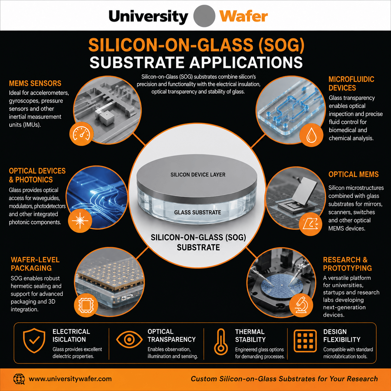
Silicon-on-Glass (SOG) substrates combine a silicon device layer with a glass wafer to create a platform well suited for MEMS, sensors, microfluidics, optical devices and semiconductor research. Researchers often choose SOG when they need the mechanical and electronic properties of silicon wafers together with the electrical insulation, optical transparency and dimensional stability of a glass substrate.
Depending on the device architecture, silicon can be bonded to borosilicate or other compatible glass substrates and subsequently thinned, patterned or etched to create the required device layer. Processes such as anodic bonding, chemical mechanical polishing (CMP), photolithography and deep reactive ion etching (DRIE) are commonly used in silicon-on-glass MEMS fabrication.
Example Silicon-on-Glass Wafer Request
A researcher at a technology startup requested a custom SOG substrate with the following specifications:
Specifications such as silicon thickness, crystal orientation, resistivity, glass composition, wafer diameter and surface finish can strongly influence device fabrication. For anodically bonded silicon-to-glass structures, the thermal expansion behavior and ionic composition of the glass are also important process considerations.
Why Use Borosilicate Glass with Silicon?
Borosilicate glasses such as Borofloat glass wafers are frequently considered for silicon-to-glass bonding because their thermal expansion characteristics are relatively compatible with silicon. This helps reduce thermally induced stress during elevated-temperature bonding and subsequent device processing.
In MEMS fabrication, the glass layer may serve as an electrically insulating support, optical window, electrode substrate or package layer. Silicon structures can then be patterned into movable elements, sensing structures, resonators, channels or other microfabricated components.
Common Silicon-on-Glass Applications
- MEMS sensors – accelerometers, gyroscopes, pressure sensors and capacitive devices
- Microfluidics – silicon microstructures combined with transparent glass for optical inspection and fluid handling
- Optical MEMS – devices requiring silicon microstructures with optical access through glass
- Wafer-level packaging – glass caps or support wafers used with micromachined silicon structures
- Research devices – custom silicon thicknesses and glass substrates for prototype semiconductor and microsystem development
Glass-based microfluidic systems are also useful when optical access is important because the transparency of glass enables direct visualization and optical detection while silicon can provide precisely fabricated mechanical or functional structures.
Silicon-on-Glass vs. Silicon-on-Sapphire
Silicon-on-Glass should not be confused with Silicon-on-Sapphire (SOS). SOS uses crystalline sapphire as the insulating substrate, whereas SOG uses a glass substrate such as borosilicate glass. Researchers requiring sapphire-based structures can review our Silicon-on-Sapphire wafers separately.
Request Custom Silicon-on-Glass Substrates
When requesting a custom SOG substrate, provide as much information as possible about your required wafer diameter, silicon thickness, crystal orientation, resistivity, glass material, glass thickness, surface finish and quantity. Additional requirements such as patterned layers, metallization, bonding, thinning or surface processing can also be included with your request.
Get Your Silicon-on-Glass Wafer Quote FAST! Submit your specifications below or Buy Wafers Online to start your research.
Why Choose Silicon-on-Glass (SOG) Substrates?
Silicon-on-Glass (SOG) combines microfabricated silicon structures with the useful electrical, optical, and mechanical properties of a glass substrate. This combination makes SOG an attractive platform for MEMS, sensors, microfluidics, optical devices, wafer-level packaging, and specialized semiconductor research.
Silicon provides a well-established material for precision microfabrication, while glass can provide electrical isolation, optical access, and structural support. The resulting substrate architecture can be particularly useful when a device requires silicon structures while also benefiting from a transparent or electrically insulating support wafer.
Silicon-to-Glass Wafer Bonding
One important method for integrating silicon with glass is wafer bonding. For suitable glass compositions, anodic bonding can create a strong silicon-to-glass interface without requiring an intermediate adhesive layer.
During anodic bonding, the silicon and glass surfaces are brought into contact at elevated temperature while an electric potential is applied across the assembly. Mobile ions in the glass migrate under the electric field, helping promote the formation of a strong bond at the silicon-glass interface.
Bond quality depends on factors such as surface cleanliness, surface flatness, glass composition, bonding temperature, applied voltage, and thermal expansion compatibility. These parameters should be considered when selecting glass for a custom SOG device.
Glass Substrate Selection for SOG
The choice of glass substrate can significantly affect processing and device performance. Researchers may consider borosilicate glass, fused silica, quartz, or other specialized glass materials depending on the required thermal, optical, electrical, and mechanical properties.
Important glass specifications can include:
- Coefficient of thermal expansion (CTE)
- Glass thickness and thickness tolerance
- Surface roughness and flatness
- Optical transmission range
- Electrical resistivity
- Thermal processing limits
- Compatibility with the selected bonding process
Silicon Device Layer Considerations
The silicon portion of an SOG structure can also be tailored for the intended experiment or device. Important specifications include silicon thickness, crystal orientation, resistivity, conductivity type, surface finish, and thickness uniformity.
Depending on the fabrication route, silicon may be bonded and subsequently thinned or patterned using established semiconductor processes such as chemical mechanical polishing (CMP), lithography, wet etching, or plasma etching.
Thin silicon device layers can be especially useful for microsystems requiring precisely defined mechanical structures or electrically active regions. Researchers should specify the final silicon thickness and acceptable tolerance when requesting custom SOG substrates.
Silicon-on-Glass for MEMS and Sensors
MEMS fabrication is one of the important research areas for silicon-on-glass structures. Silicon can be patterned into micro-scale mechanical components while the underlying glass provides support and electrical isolation.
Depending on the device design, SOG structures may be investigated for capacitive sensors, pressure sensors, inertial devices, resonators, microactuators, and other micromachined systems. Glass may also support patterned electrodes or provide optical access to the silicon structures.
Learn more about substrates used for MEMS fabrication and other microfabrication applications.
SOG for Microfluidics and Optical Devices
Glass transparency can make silicon-on-glass structures useful for devices that require optical inspection, illumination, imaging, or optical detection. This can be valuable in microfluidic and lab-on-chip research where researchers need to observe structures, particles, or fluids through the substrate.
SOG architectures may also be investigated for optical MEMS, photonic structures, biosensors, and integrated microsystems where silicon microfabrication is combined with a transparent support material.
Silicon-on-Glass vs. Silicon-on-Insulator
Although both technologies provide silicon device layers with electrical isolation, Silicon-on-Glass (SOG) and Silicon-on-Insulator (SOI) are different substrate architectures.
Conventional SOI wafers typically contain a crystalline silicon device layer separated from a silicon handle wafer by a buried silicon dioxide layer. SOG instead integrates silicon with a glass substrate. The glass can provide substantially different optical, electrical, thermal, and mechanical characteristics from a conventional silicon handle wafer.
The appropriate platform depends on the device architecture, fabrication process, required silicon thickness, optical requirements, electrical isolation, thermal budget, and packaging strategy.
Choosing SOG Specifications for Your Research
Researchers requesting custom Silicon-on-Glass substrates should provide detailed specifications whenever possible. Useful information includes:
- Wafer diameter
- Silicon device-layer thickness and tolerance
- Silicon crystal orientation
- Resistivity and conductivity type
- Glass material and thickness
- Surface finish and roughness requirements
- Bonding or processing requirements
- Quantity
UniversityWafer supplies silicon wafers, glass substrates, and custom research wafer specifications for universities, laboratories, startups, and semiconductor development programs.
Related Silicon-on-Glass Resources
- Silicon Wafers – Silicon substrates available in multiple diameters, orientations, resistivities, and surface finishes.
- Glass Wafers & Substrates – Explore glass substrates for MEMS, microfluidics, optics, sensors, and wafer bonding.
- Borofloat Glass Wafers – Borosilicate glass substrates for research, microfabrication, and silicon-to-glass bonding.
- Wafer Bonding – Learn about wafer bonding techniques used to integrate silicon and other substrate materials.
- Silicon-on-Insulator (SOI) Wafers – Compare SOG with silicon device layers isolated by a buried oxide layer.
- MEMS Substrates – Silicon and specialty substrates for sensors, actuators, resonators, and microsystems.
- Microfabrication – Substrates and processes for developing micro-scale semiconductor and MEMS structures.
- Chemical Mechanical Polishing (CMP) – Wafer planarization and surface preparation for advanced substrate fabrication.