Why is it so hard & expensive to control the TTV under 0.5 µm?
Looking for Si wafer that has Thickness Control of 1.0mm +/- 0.5um
UniversityWafer, Inc. offers the world's thinnest silicon wafers with a Total Thickness Variation (TTV) of one micron. Our high quality silicon wafers are perfect for your next semiconductor device fabrication project.
For 3" or 4" wafers we can achieve TTV<0.5µm (with 3mm edge exclusion), for either lapped, or ground or double-side-polished wafers, but it is expensive.
Get Your LOW TTV on Silicon Quote FAST! Buy Online and Start Researching Today!
To achieve absolute thickness of 1,000.0±0.5µm is another matter.
We would have to agree on a common calibration standard.
We cannot achieve Bow/Warp<0.5µm. It is impossible to measure these parameters with such precision.
For 3"Ø and 4"Ø wafers we can certainly achieve Bow<5µm, Warp<10µm.
Anything less would require careful definition of how these parameters would be measured.
The above conversation was a question and answer session between our engineer and a research client.
The Total Thickness Variation of a Silicon Wafer and Its Applications
The Total Thickness Variation (TTV) of a silicon wafer is a measurement of the maximum difference in the 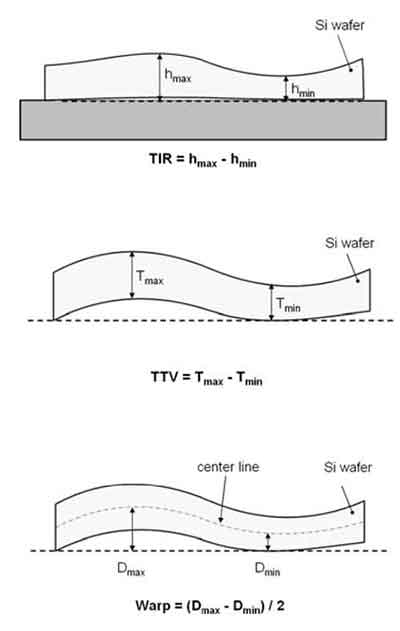 thickness of the entire wafer. This is typically measured at five locations on the wafer and the maximum difference is calculated. Ultimately, this figure is the basis for determining the quality of the silicon wafer. In practice, the GTIR is generally less than 1um. However, there are several other factors that must be taken into consideration.
The first factor to consider is the Bow. The Bow is the locus of points on the wafer that are equidistant between the front and back surfaces. It is calculated by calculating the deviation from the median surface. The center point is the point that is most deviated from the median surface. The remaining two points are evenly spaced apart. This means that the bow is the average of the three measurements.
The Total Thickness Variation of a silicon wafer is a very important measurement. TTV measures the differences between the minimum and maximum thicknesses measured on the wafer. The TTV increases with the polishing process. In other words, the less variation there is in the total thickness, the lower the TTV. The bow is also a measure of the width of a silicon wafer, but not necessarily of its depth.
In addition to TTV, the Bow also determines the MRR. In fact, the Bow is the concavity of a silicon wafer, measured from its center. TTV is also called the bow. A good bow is less than 30 um. The bow is the fundamental reason for silicon wafer rejection. There are several types of defects, and even so-called prime wafers can have defected surfaces.
The RPDmax is the maximum distance above or below the reference plane. Warp is always a positive value. For a single-crystalline silicon wafer, the median surface intersects the reference plane at the center. If there is any bowing, the warp value would be zero. In addition, the RPDmin and the RPDmax values indicate the shape of a silicon wafer. The measured values are then compared with the SEMI standard.
The RPDmax is the maximum distance above or below the reference plane. The warp measurement is always positive. If the wafer is perfectly circular, then the RPDmax and RPDmin values should be equal. Then, the RPDmax and RPDmin are the maximum height above or below the reference plane. In the case of a circular silicon wafer, the warp is always positive. The higher the resistance, the more irregular the shape of a silicon-based device.
The total thickness variation of a silicon wafer is a measure of the total thickness of a single silicon wafer. If it is greater than this value, it is n-type. P-type, on the other hand, is the opposite. If there is too much variation in a single wafer, the material is categorized as p-type. If it has a p-type, the electrons are negatively correlated.
The total thickness variation of a silicon wafer is a measure of the thickness variation of the entire wafer. It can be as thin as 10mm or it can be more than 10mm. When it is thicker than this, it is not a prime. As a result, it is not suitable for electronic devices. But there are other types of thickness variations. If a wafer is too thick, it is not a prime.
Another factor to consider when considering the total thickness variation of a silicon wafer is its shape. Some silicon wafers are thinner than others. This means that the total thickness variation of a silicon-based wafer is not uniform throughout the entire wafer. The thickness variation of a silicon-based waffle affects IC patterns in many ways. It can also impact the quality of a semiconductor. A thicker and more uniform silicon-based wafer will result in a higher quality IC.
Another important factor to consider is the resistance to movement of electrons and holes in silicon. This value is directly related to the voltage across the silicon wafer. It is measured in Ohmcm, and can be used to compare the resistivity of various materials. Heavy-doped material has a low resistivity. Its resistivity will be affected by the amount of impurities in the silicon. For this reason, it is essential to carefully select the processing method for the silicon wafers that you use.
Why is it so to Control the Total Thickness Variation (TTV) under 0.5 µm?
Total Thickness Variation TTV is a measure of flatness. It is the difference between thickest and the thinnest portion of the wafers. It is harder to make a wafers that has a TTV<5µm than it is to make one that is TTV<10µm. It is harder still to make TTV<1µm. It is harder still to make TTV<0.5µm. It is harder still to make TTV<0.05µm. And so on. If it was easy to make TTV<0.5µm then that would be the standard. It is not easy and so the standard is <10µm. Please confirm that you understand this concept that tighter specifications are harder to achieve and thus more expensive.
1,000.0±0.5µm means that all of the wafers when measured have a center point thickness of 1,000µm with a 0.5µm tolerance. So, every wafer will be in the range of (999.5-1,000.5). The standard range is ±25µm (975-1,075). It is more difficult to make ±10µm. It is even more difficult to make ±5µm. More difficult to make ±1µm. Even more difficult to make ±0.5µm. Please confirm that you understand of a lower thickness tolerance is harder to achieve and thus more expensive.
We can do much better than SEMI standard for Bow/Warp. Standard is <40µm and we can do Bow<5µm and Warp<10µm. There are limits to what can be made and measured.
We do have a large selection of 1 micron TTV substrates