
Silicon Wafers for Equipment Testing & Reclaiming
UniversityWafer supplies 200mm (8") and 300mm (12") silicon wafers for semiconductor equipment testing, process qualification, reclaiming, and tool development. These low-cost wafers are ideal for equipment setup, dummy runs, wafer handling verification, robotic testing, process calibration, and manufacturing line qualification.
Available inventory may include bare wafers, patterned wafers, film-coated wafers, polished wafers, and reclaim wafers. Pricing depends on wafer type, quantity, and current inventory.
Get Your Equipment Testing Wafer Quote FAST! Or, Buy Online and start testing today!
200mm (8") Silicon Wafers
Our 200mm silicon wafers are commonly used for semiconductor equipment qualification, process development, reclaim operations, and wafer handling verification.

200mm Reclaim Silicon Wafers
Reclaim wafers provide a cost-effective solution for equipment setup, robot teaching, cassette qualification, deposition trials, and process optimization without consuming expensive prime wafers.

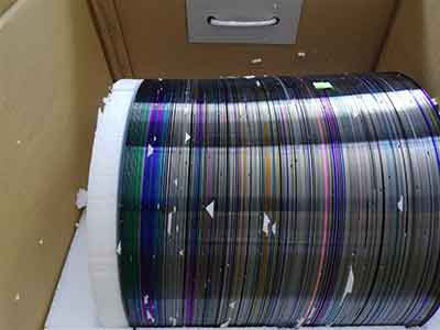
300mm (12") Mixed Coin Roll Wafers
Mixed coin roll wafers are frequently purchased for equipment testing, reclaiming, training, and semiconductor manufacturing process development.
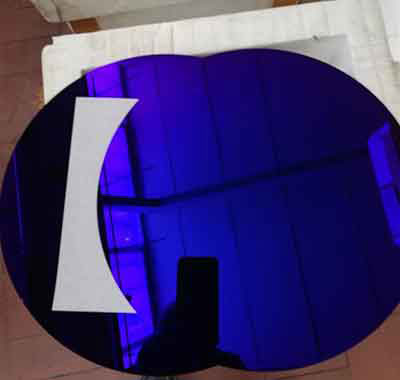
300mm Patterned Silicon Wafers
Patterned 300mm silicon wafers are suitable for testing semiconductor manufacturing equipment, validating automated wafer handling systems, and evaluating process performance under realistic production conditions.
Silicon Wafers for Testing Semiconductor Equipment
Silicon wafers for equipment testing are used to qualify semiconductor tools, verify wafer handling systems, test process stability, and support reclaim operations. These wafers are often lower-cost than prime device wafers and are commonly used for setup, calibration, dummy runs, process checks, and equipment development.
UniversityWafer supplies 200mm and 300mm silicon wafers for semiconductor equipment testing, reclaiming, process development, thin-film testing, and wafer handling evaluation. Available inventory may include bare wafers, patterned wafers, film wafers, polished wafers, etched wafers, and mixed coin roll wafers.
Why Use Test or Reclaim Silicon Wafers?
Test wafers and reclaim wafers help engineers run process checks without using expensive prime grade material. They are useful for validating tools used in deposition, etching, cleaning, inspection, metrology, lithography, wafer handling, and automated test equipment.
- Lower-cost wafers for equipment setup and process testing
- Useful for semiconductor tool qualification and calibration
- Available in 200mm and 300mm diameters
- Options may include bare, patterned, polished, film, and etched wafers
- Suitable for reclaiming, dummy runs, and wafer handling tests
Common Applications
Equipment testing wafers are commonly used by semiconductor fabs, universities, equipment manufacturers, process engineers, and research labs. They help confirm that wafer tools can load, transfer, clamp, spin, heat, cool, inspect, deposit, etch, or measure wafers correctly before valuable production wafers are processed.
Reclaim wafers are also used when a wafer can be cleaned, polished, or reused for non-device applications. This helps reduce cost while still providing a realistic silicon substrate for process and equipment testing.
Available Equipment Testing Wafer Inventory
The following wafers are examples of materials used for semiconductor equipment testing and reclaiming. Availability and price depend on quantity, diameter, surface condition, and current inventory.
| Item | Product | Type | Diameter | Notch | Thickness | Front | Back | Quantity (kg) |
|---|---|---|---|---|---|---|---|---|
| 1 | 8" Pattern Wafer | P/N | 200 ± 0.5mm | SEMI standard | Avg. 700-900µm | Pattern | Etch or film | 313 |
| 2 | 12" Bare/Film Wafer | P/N | 300 ± 0.5mm | SEMI standard | Avg. 680-750µm | Polish or film | Polish or film | 221 |
Price depends on quantity.
Product: 12" mixed coin roll wafers are also available for reclaiming and equipment testing applications.
Order Silicon Wafers for Equipment Testing
UniversityWafer can help you source low-cost silicon wafers for testing semiconductor equipment, qualifying tools, reclaiming, and process development. Send us your required diameter, wafer type, thickness, quantity, and surface condition for a fast quote.