
I am required a Barium Hexaferrite 2-inch Sputtering Target  without a copper backing plate and with a very high density so we can also use this in Laser ablation in PLD. Please provide us with the quote of the target and estimated delivery time. We need a 2-inch Diameter and 0.25 mm thick highly dense Barium Hexaferrite target.
How We Help Researchers
A graduate research student requested the following:
UniversityWafer, Inc. Quoted:
Barium Hexaferrite:99.99% purity,BaFeO3,dia 2“*5mm
Reference #278010 for specs and pricing.
Get Your Quote FAST! Buy Substrates Online and Start Researching Today!
What does a Sputtering Target Look Like?
Sputter targets are commonly rectangular or circular. Other shapes  can also be produced. For example Gold (Au) sputting targets can be made in different shapes and even be oddly shaped depending on the type of thin layers to be produced. Typically, the heterogeneity of these sputter targets results in a "sputterfilm" that does not have the uniformity desired for most semiconductor and photoelectric applications.
Please let us know of your needs!
The sputtering target market is driven by the increasing demand worldwide and is therefore a key driver for the development and development of new technologies in the glass industry. Manufacturers use sintering technology such as sintered glass and deeply processed glass to produce their increased sputtering targets. Some companies, in particular deep-glass companies and glass manufacturers, are concentrating on expanding their coated glass production lines. [Sources: 6, 9]
The target market for sputter products can be divided into three main categories depending on the material: glass, glass products and glass components. These products include sputtering and sputtering targets as well as their components and their applications in the glass industry. [Sources: 2, 6]
In some cases, manufacturers will create segmented targets linked by special joints, but some sputtering plants will require larger sputtering targets. The most important metals used in the production of conductive layers are: AEM deposition, which forms a barrier layer between the surface of the target material and the conductive layer (the material itself). These are used as barrier layers and include a range of target materials used for coatings and industrial tools. They can also be embedded with a variety of other materials such as ceramics, polymers, metals, plastics and other metals. [Sources: 0, 3, 8]
In many cases, used or scrapped tantalum targets are not used directly by tantalum metal producers to produce new ingots or blanks for stuttering target producers, but by scrap traders, particularly Exotech, which pays prices for their use. For this reason, the price paid by the manufacturer of a sputter target for a used TantAlum target is higher than the price paid for Tant aluminium scrap by a sputter target manufacturer. The high prices of Tant Alu are therefore paid for the tantalum targets used by their scrap buyers such as Ex techo, and also for the higher prices of the targets themselves, where they are used as ore substitutes. [Sources: 13]
In order to deposit a film with high integrity during reactive sputtering, low-oxygen metal powders are required, which consist of metal powder produced by other metal parts. Sputtering targets are relatively expensive to make precious metals electrophile, requiring several refining steps. [Sources: 7, 10, 12]
Proper processing can produce powders that meet the tantalum of a sputtering target that has a higher electrical conductivity than the ingot in which it is located. Sputting targets are thin layers that are grown from material by sputtering. They are used in the production of high-performance electronics, electronic components and other materials. These targets can be manufactured by processing metals and ceramics or used for other purposes, such as the manufacture of electronic components. [Sources: 3, 7, 11]
As mentioned above, two types of targets are used, with the magnetron sputtering method used for TCO separation and cold spraying. Cr - CrO 2 targets have traditionally been used to form black matrices for flat panel displays that have no health or environmental concerns. Cold spraying is also used in some cases to coat large areas, as the sputtering targets currently used, which are formed using conventional manufacturing methods, tend to be too small for many applications. Moreover, most sputtering target materials are metallic elements and alloys, although there are ceramic targets that produce thin coatings hardened with various tools. [Sources: 1, 4, 8]
[Sources: 1, 8, 9]
The thickness of the target carrier material can be the appropriate thickness used to form the sputtering target. SputterTargets and carrier plates can also be used in a variety of other applications such as semiconductor and photoelectric applications. There are a number of different types of carrier targets that can be used to produce sputter targets and other materials. [Sources: 7]
The powder used to produce the resulting metallurgical article may have a purity vis-à-vis the metal. The ions used for bombarding the sputterer are also embedded with MoO 3 films, which generate reactive sputtering (Mo) in the target. This creates a decent thin film and a very high degree of purity of the material. [Sources: 1, 7, 8]
Molybdenum sputter targets are a competent area in the coating industry in terms of precise coating during sputtering. There is a wide range of applications for sputtertargets, but the most common applications range from high-performance coatings for industrial applications to the production of high-quality ceramics and other materials for the automotive industry. [Sources: 5, 9]
The growing demand for stuttering targets and the increasing use of high-performance electronics in the automotive industry have boosted APAC's targeted market revenues. The growth of integrated circuits and other advanced technologies such as smartphones and tablets has created an inflow of demand for the stuttering Asia-Pacific targeting market. [Sources: 9]
What are Sputter Targets?
Sputtering targets are thin discs or sheets of a material that are used in a process called sputtering to deposit thin films of the material onto a substrate like a silicon wafer.. Sputtering is a process in which atoms of the target material are physically ejected from the surface of the target and deposited onto a substrate, typically by bombarding the target with ions.
Sputtering targets have a wide range of applications in various fields, including microelectronics, thin film solar cells, optoelectronics, and decorative coatings.
In microelectronics, sputtering targets are used to deposit thin films of materials such as aluminum, copper, and titanium onto silicon wafers to create electronic devices such as transistors, diodes, and integrated circuits.
In thin film solar cells, sputtering targets are used to deposit thin films of materials such as cadmium telluride, copper indium gallium selenide, and amorphous silicon onto a substrate to create solar cells with high efficiency.
In optoelectronics, sputtering targets are used to deposit thin films of materials such as indium tin oxide and aluminum zinc oxide onto a substrate to create transparent conductive coatings for LCD displays and touch screens.
In decorative coatings, sputtering targets are used to deposit thin films of materials such as gold, silver, and chrome onto a variety of substrates to create decorative coatings for automotive parts, jewelry, and other products.
Overall, sputtering targets have a wide range of applications in various fields due to their ability to deposit thin films of materials onto a variety of substrates with high precision and uniformity.
Below are just some of the sputtering targets that we have:
Item |
Specification |
Quantity |
1 |
CST-01-Cobalt Sputtering target Cobalt (Co),Purity:99.95%:Diameter: 1inch, thickness: 0.125inch |
1 No. |
2 |
AKN-NiFe-Ni80Fe20 Ni80Fe20 sputter target,Purity:99.95%:Diameter: 2inch, thickness: 0.125inch |
1 No. |
3 |
AKN-NiFe-Oneinch-Ni80Fe20 Ni80Fe20 sputter target,Purity:99.95%:Diameter: 1inch, thickness: 0.125inch |
1 No. |
4 |
AKN-WS2-WS2 Ws2 sputter target,Purity:99.9%:Diameter: 1inch, thickness: 0.125inch, with Cu backing plate |
1 No. |
5 |
AKN-Gd2O3-Gd2O3 Gd2O3 sputter target,Purity:99.9%:Diameter: 1inch, thickness: 0.125inch, With Cu backing plate |
1 No. |
What Are Sputtering Targets Used For?
Sputtering targets are metallic objects used in sputtering processes. Depending on the application, they can range from one-inch squares to more than a yard in length. While the smaller sputtering targets are often less than a centimeter in diameter, larger targets are required for some equipment. The sputtering process requires a metal target to be segmented into a specific shape and size.
 A sputtering target is used to deposit thin films by PVD. Its atoms are pulled from a substrate and collide with the metal target to form a thin film. These atoms are condensed into a gas and eventually harden into a thin film. The thin film is then deposited. The process of sputtering is highly accurate and is an ideal tool for producing precision products.
Traditionally, sputtering targets are rectangular or circular. Today, they have become more specialized and can be manufactured into any shape. In addition to these traditional shapes, many target suppliers are able to create a special shape for their customers. The rotational target offers more precise thin film deposition and is shaped like a long cylinder. A rotating sputtering target has greater surface area and faster deposition.
Sputtering targets have many uses, including thin film deposition. The technique is relatively simple and involves a target that has a specific composition. The material sprayed onto the target is then transferred to the substrate and dries to produce the thin film. The final product is a thin film that has been shaped and patterned in a variety of ways. This process is known as the sputtering of a film.
In the process of thin film deposition, sputtering targets are used in vacuum coating equipment. The process of PVD allows a thin film to be formed by transferring electrons between atoms. This process is known as sputtering. The process requires the use of a target that is designed to be flexible and rigid. A rotating sputtering target is more efficient and has higher yield.
While sputtering systems are able to use a wide variety of materials, there are certain materials that are not compatible with sputtering. For example, the melting point of the target determines how conductive the material is. Some sputtering targets are non-conducting and should be coated with a protective material. However, some targets are non-conductive, and should be avoided for these reasons.
A thermal sputtering target is a sputtering device that uses a metal target. Its purpose is to coat a thin film layer of a material with a PVD atom. The heat generated by the target's sputtering process causes the metal to bond with the substrate, thereby forming a thin film. The result is a thin film.
The sputtering process can produce valuable materials. Typically, the sputtering targets are made of precious metals. Using a sputtering machine, aluminum can be deposited onto the substrate. The resulting metal is then referred to as the "target". This process is called sputtering. With the proper sputtering apparatus, a metallic target is coated with a thin layer of a PVD material.
A sputtering target is a thin layer of material that is deposited onto a substrate. Unlike conventional sputtering equipment, sputtering targets can be either metallic or nonmetallic. They can also be bonded together with other metals for added strength. In addition to sputtering, these devices can be etched or engraved, which makes them perfect for photo-realistic imaging.
As far as the process is concerned, sputtering targets are often used to produce thin films. For example, sputtering of semiconductors involves the use of metallic alloys. In semiconductors, sputtering is commonly used to form conducting layers. For this reason, sputtering targets must be able to guarantee chemical purity and metallurgical uniformity.
Silicon Sputtering Target
A silicon sputtering target is made by sputtering of the metal from a Si ingot. The targets can be  manufactured by various processes and methods, including electroplating, sputtering, and vapor deposition. The preferred embodiments further provide additional cleaning and etching processes to achieve desirable surface conditions. The resulting targets are highly reflective, have a roughness of less than 500 Angstroms, and are relatively quick to burn. The films produced by such a silicon target have low particle counts.
Silicon sputtering targets are used to deposit thin films on silicon-based materials. They are commonly used in displays, semiconductors, optics, optical communication, and glass coating applications. They are also suitable for etching high-tech components. The N-type silicon sputtering target is available for different purposes. It is suitable for applications in many fields, including electronics, solar cells, semiconductors, and displays.
A silicon sputtering target is a sputtering device used to deposit a material onto a surface. Typically, it is composed of silicon atoms. The sputtering process requires a precise amount of material, which can be a large challenge. Using an ideal sputtering device is the only way to make a silicon-based component. It is important to note that the sputtering process does not use a silicon sputtering target.
What is the Optical Or Stress Data for Sputtering Silicon Wafers?
One of the most common questions about sputtered Silicon is what is the optical or stress data. While we 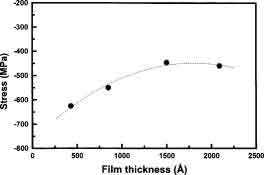 don't have data on diode-sputtered films, we can determine how the film responds to a high-stress level and which microstructure is best suited for the desired application. For example, we can observe the stress-thickness relationship in the films based on their thickness and resistivity.
In general, sputtered silicon exhibits compressive stress. It shows an enhanced surface diffusion due to the high substrate temperature. However, the enhancement is not large enough to form a nc phase and compensate for the difference in kinetic energy. The stress data provided are useful for determining the optimum deposition conditions for a silicon film. The Thornton model is one example of a method for determining the optimal deposition conditions.
The first step is to determine the working pressure of the substrate. At low working pressures, amorphous silicon exhibited a low mechanical loss, and when heated to high temperatures, the mechanical loss increased. In addition, the working pressure changed the RMS values, resulting in rougher films with columnar microstructure. This was in agreement with Thornton's structure zone model. This model has several advantages.
The second step is to determine the substrate temperature. The temperature of the substrate during the initial process is too high. Therefore, the Pt-sputtered silicon would poison the Si. The diffusion barrier would not hold for the Pt-sputtered silicon. Therefore, the underlying silicon would have no insulating properties. This would reduce the energy requirements for the device processing. In other words, it is important to determine the working temperature of the silicon substrate.