
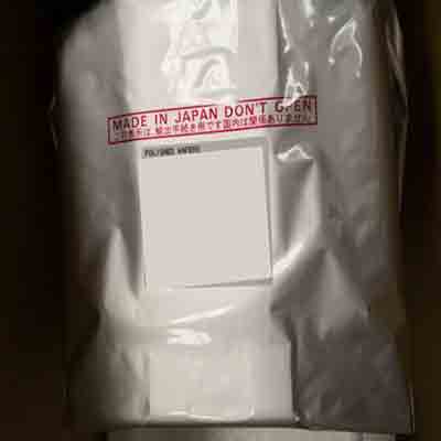
6 Inch and 8 Inch SUMCO Wafers
The prices are per wfer for 25 wafers. You may be able to buy more wafers for a lower cost. Please let us know what quantity you would like.
6 Inch $39.90 each
8 Inch $47.90 each
Get Your Quote FAST! Or, Buy Online and Start Researching Today!
According to a recent survey, the global market for large silicon wafers (LSA), the largest semiconductor market in Europe and North America, has reached US $xx and is growing at an annual rate of 2.5% to 3%. [Sources: 8]
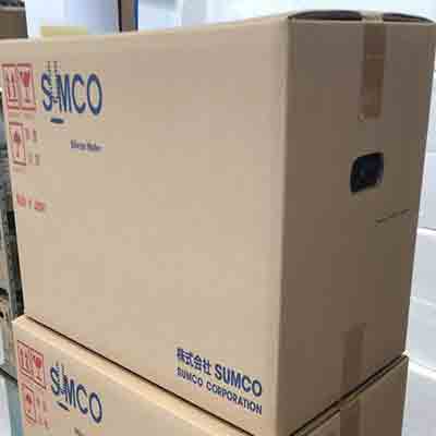
SUMCO Silicon Wafers
SUMCO is a leading supplier of high-quality silicon wafers. The company has several proprietary technologies that have advanced the manufacturing process. These products are designed to meet the demanding requirements of the semiconductor industry. For example, SUMCO's highly-doped crystals and epi wafers achieve sub-micron level flatness and ultra-clean surfaces. Additionally, SUMCO provides the highest quality of products.
These semiconductor devices are used in nearly every aspect of our lives, providing the technological foundation for many different electronic products. Ultimately, the quality of silicon wafers is critical to our standard of living. As such, SUMCO is committed to sustainability, CSR, and corporate governance. For instance, it recently named Hemlock Semiconductor as its supplier of the year. The company focuses on these three areas to promote corporate social responsibility.
In addition to high-quality silicon wafers, SUMCO also provides a variety of services. The company has two manufacturing facilities in the United States and employs about 500 people. In addition, SUMCO also offers worldwide inventory management and product delivery. SUMCO's Internet-based customer information system helps customers get detailed technical information about their orders. Regardless of the size of a company's business, SUMCO has a range of solutions to meet the needs of its customers.
SUMCO produces a variety of epitaxial silicon wafers for a wide range of industries. Its offerings include silicon on insulator (SOI), power discrete, CMOS, and power-diode. SUMCO provides polished wafers for the semiconductor industry. The semiconductor industry is a global marketplace and SUMCO's high-quality silicon wafers are a key ingredient to the success of any semiconductor project.
SUMCO is a leading supplier of silicon wafers. SUMCO offers a range of products ranging from epitaxial to n-type. Various SUMCO silicon wafer types are available in varying sizes and geometries. SUMCO provides a complete array of solutions to suit your requirements. The company is also a leader in the manufacturing of epitaxial silicon wafers.
SUMCO is a leading supplier of epitaxial silicon wafers. Its products are used in power discrete and CMOS applications. Its n-type and p-type epitaxial wafer products are also available. Its polished wafers are a great choice for a variety of industries. They can also be used for power semiconductors. Despite the wide array of applications, SUMCO silicon wafers offer a variety of benefits for the end consumer.
SUMCO is an industry leader in manufacturing and supplying semiconductor grade silicon wafers. The company is a leading manufacturer of silicon wafers for the semiconductor industry. Its high-quality wafers are used in a variety of electronics, from smartphones to televisions. A variety of CMOS applications are fueled by SUMCO silicon wafers. They are used to power a variety of electronic products.
SUMCO also manufactures SOI and n-type silicon ingots. These are the best choice for power-dense and high-speed discrete applications. In addition, SUMCO can produce polished wafers. All three types of silicon wafers are available. SUMCO is one of the few companies that can provide these products. The company offers an assortment of quality products and services for its customers.
SUMCO uses the Electromagnetic Casting Method to mass-produce silicon wafers at high yield. Its customers need high-quality, high-performance solar cells for their projects. This technology can be produced at SUMCO's production volume in just a few days. The company also offers other advantages such as high yields, including improved efficiency. This is why SUMCO has a global presence and is a trusted supplier of these products.
SUMCO has a variety of proprietary technologies. For example, the company uses the latest proprietary technology from Japan and the United States to produce semiconductors. In addition to this, SUMCO silicon wafers are also used in memory chips to store data. This technology is crucial for creating a number of electronic products, such as mobile phones, computer monitors, and other electronic gadgets. This type of material has many uses in electronics, and SUMCO is committed to meeting these needs and expectations.
SUMCO offers to sell silicon wafers to Samsung Austin Semiconductor. The company manufactures the wafers according to the specifications of Samsung, and e-mails Samsung engineers with test results to secure shipment authorization. In addition to this, SUMCO also provides product support to Samsung Austin, which the company does not want to purchase without it. There's a high possibility that the accused wafers were sold under an unlicensed environment.
150mm and 200mm SUMCO Substratate Sale
We have the following specials on sumco wafers. Please let us know what you can use. If you cannot, please let us know if you can use another specification/quantity.
Please ask for the Excel File of the Inventory.

Sumco Silicon Wafers
The semiconductor market for silicon wafers will be significantly affected in the 2020s and the impact of
The above described silicon wafers are manufactured using the above described process, whereby the silicon wafer is manufactured according to the present invention. Thermal annealing suppresses the formation of slip and provides the void that the silicon wafer according to the present invention has in it and, if the surface of the silicon wafer is nitride, an empty material is injected into it. Then, through the subsequent thermal ageing, we obtain a quality silicon wafer with a double-layer in which the same number of vacancies are present as in the silicon wafer layer. To produce the silicon wafers described above, the methods described above are used in combination with the following methods. [Sources: 4, 6]
By irradiating a predetermined amount of silicon atoms into phosphorus atoms, the neutrons in the silicon ingots can be obtained to produce a silicon wafer with constant resistance. By using the methods described above to produce silicon discs from nitrogen - doped nitrogen doping in silicones - the size of COPs was significantly reduced to small children. COP defects exist in all silicone wafers obtained using the methods described above. [Sources: 4]
In an IGBT, the resistance does not change, but it does change when subjected to different heat processes that correspond to the heating steps in the IGBT production process. This affects the recombination life span, which can lead to a reduced recombination life span. In order to use a silicon wafer in its IBBT, it is necessary to reliably inhibit the effects of the heat history that can be caused by the recombination of the lifetime, in order to reduce them. For I GBTs, if you examine the different thermal histories corresponding to each heating step of the production processes of IBTG, then the resistance will change. [Sources: 4]
The number of tiny particles that adhere to the surface of the silicon wafer must be as close as possible to zero. After the free spaces (n-2) decompose at high temperature, they are injected into the silicon wafers to form Si - n - y nitride layers on the surfaces of silicon wafers. When activated, the plasmatic nitrite gas further accelerates the formation of Si-N-Y nitrides on the surface of a silicone wafer, resulting in a shortening of the recombination life of I-GBTs. While the nitrate gas was activated and accelerated by the presence of an ionic gas (N-1) and then a nitrogen gas. [Sources: 1, 6]
This example is explained next, and a reference to FIGS explains the formation of Si - n - y nitride layers on the surface of silicon wafers. [Sources: 6]
The schematic cross-sectional view showing the formation of Si - n - y nitride layers on the surface of silicon wafers is below. 1 is an example of the production method on a silicone wafer, which is carried out by using a liquid gas with high temperature, low pressure oxygen (LIGO). [Sources: 6]
A 200 mm silicon wafer is used to manufacture ICs, and the product line has been expanded to include particle and machine manufacturing for high-performance silicon chips. [Sources: 2]
Semiconductor functions have evolved over the years and SUMCO has invested heavily in technological advances to deliver customers the best silicon wafer products in their class. All our semiconductor products are manufactured with our silicon wafers, with an emphasis on high quality, high performance and low cost. [Sources: 1, 5]
Sources:
[0]: https://www.globalmarketmonitor.com/report_blog/408742-Semiconductor_Material__Silicon_Wafer.html
[1]: https://www.marketscreener.com/quote/stock/SUMCO-CORPORATION-6498180/news/Sumco-CSR-Report-2017-24475169/
[2]: https://www.universitywafer.com/silicon-wafer-diameters.html
[3]: https://semiengineering.com/mixed-outlook-for-silicon-wafer-biz/
[4]: https://www.google.com/patents/US20070000427
[6]: https://patents.google.com/patent/US20050130452
[7]: https://english.etnews.com/20171114200001
[8]: https://www.benzinga.com/pressreleases/20/04/ab15799021/semiconductor-large-silicon-wafer-2020-global-industry-size-share-trends-key-players-analysis-app
[9]: https://blog.semi.org/business-markets/tough-times-for-silicon-wafer-market-continue-after-two-consecutive-quarters-of-revenue-decline
Related Silicon Wafer Resources
- Silicon Wafers – Prime, Test & Mechanical Grades
- Test Grade Silicon Wafers for Process Development
- Epitaxial Silicon Wafers
- Silicon-on-Insulator (SOI) Wafers
- Czochralski-Grown Silicon Wafers
- Single Crystal Silicon Ingots
- Silicon Wafer Diameter Guide
- Semiconductor Fabrication Technology
- Solar Silicon Wafers
- Silicon Wafer Sorting & Testing