“Our research group is primarily interested in wafer flatness and cleanliness for spin coating and UV lithography. If the test-grade wafers do not meet our surface requirements, we will likely purchase prime-grade wafers.”
Reference #267793
UV lithography (photolithography) is a core microfabrication method used to pattern photoresist and transfer features onto a wafer during semiconductor, MEMS, and lab-on-chip processes. Depending on your toolset, you may use DUV (e.g., 248 nm or 193 nm) or EUV (13.5 nm) exposure to define critical dimensions. Wafer selection matters too—flatness (TTV), cleanliness, and surface quality help improve resist coating uniformity, focus control, and repeatability during exposure and development.

UniversityWafer supplies silicon wafers for UV lithography, photolithography, MEMS fabrication, microfluidics, semiconductor research, and university cleanroom processing. Researchers can select test-grade silicon wafers , prime-grade silicon wafers , silicon-on-insulator (SOI) wafers , and custom substrates based on the surface quality, flatness, thickness, film stack, and device requirements of the lithography process.
The best wafer choice depends on factors such as resist thickness, exposure-tool handling, alignment requirements, backside processing, feature size, and whether the substrate will later undergo etching, implantation, oxidation, deposition, or lift-off.
Silicon substrates for photolithography can be specified by parameters such as:
Prime-grade wafers are generally preferred when the process requires tighter control of surface quality, flatness, defectivity, or dimensional uniformity. They are commonly used for critical lithography, device fabrication, and processes where focus and overlay performance are important.
Test-grade wafers can be a lower-cost option for process development, equipment qualification, photoresist testing, spin-coating trials, training, and other applications that do not require prime-grade specifications.
The grade alone should not determine suitability. Researchers should compare the actual TTV, bow, warp, surface finish, particles, edge condition, and other relevant specifications with the requirements of the lithography tool and process.
SOI wafers are frequently used when lithography is part of a MEMS, silicon-photonics, sensor, or advanced device process. The device layer provides a controlled crystalline silicon thickness while the buried oxide provides electrical isolation and can support specialized etching strategies.
Thermal oxide silicon wafers are also useful for lithography when an electrically insulating SiO2 layer, defined dielectric thickness, optical contrast, or patterned oxide structure is required.
Get Your UV Lithography Wafer Quote FAST!
Or,
Buy Silicon Wafers Online
and Start Researching Today!
A research fellow requested guidance on selecting silicon wafers for spin coating and UV lithography, with particular emphasis on surface cleanliness, flatness, and wafer quality.
“Our research group is primarily interested in wafer flatness and cleanliness for spin coating and UV lithography. If the test-grade wafers do not meet our surface requirements, we will likely purchase prime-grade wafers.”
Reference #267793
For this type of application, comparing actual wafer specifications is more useful than relying only on the grade designation. Parameters such as TTV, bow, warp, polish quality, particle contamination, and surface roughness can all affect resist coating and exposure performance.
Lithography depends on maintaining a controlled relationship between the wafer surface, photoresist film, photomask or projected image, and focal plane. Variations in wafer geometry or surface condition can influence resist uniformity, focus, alignment, overlay, and pattern transfer.
A useful starting point is to match the wafer to the process rather than automatically selecting the most expensive grade.
Silicon and silicon-based substrates patterned by UV lithography are used across many research and manufacturing areas, including:
UV lithography, commonly called photolithography , is a patterning process used to define microscopic features on semiconductor wafers and other substrates. A photosensitive resist is coated onto the substrate and selectively exposed to ultraviolet light through a photomask or projection system.
After development, the patterned resist acts as a temporary mask for later processing steps such as etching, ion implantation, oxidation, metal deposition, dielectric deposition, or lift-off. Repeating lithography and pattern-transfer steps enables fabrication of integrated circuits, MEMS devices, sensors, microfluidic structures, photonic components, and other microfabricated devices.
A typical UV photolithography process combines wafer preparation, photoresist coating, exposure, development, and pattern transfer. The exact sequence depends on the resist system, exposure tool, substrate, and downstream fabrication process.
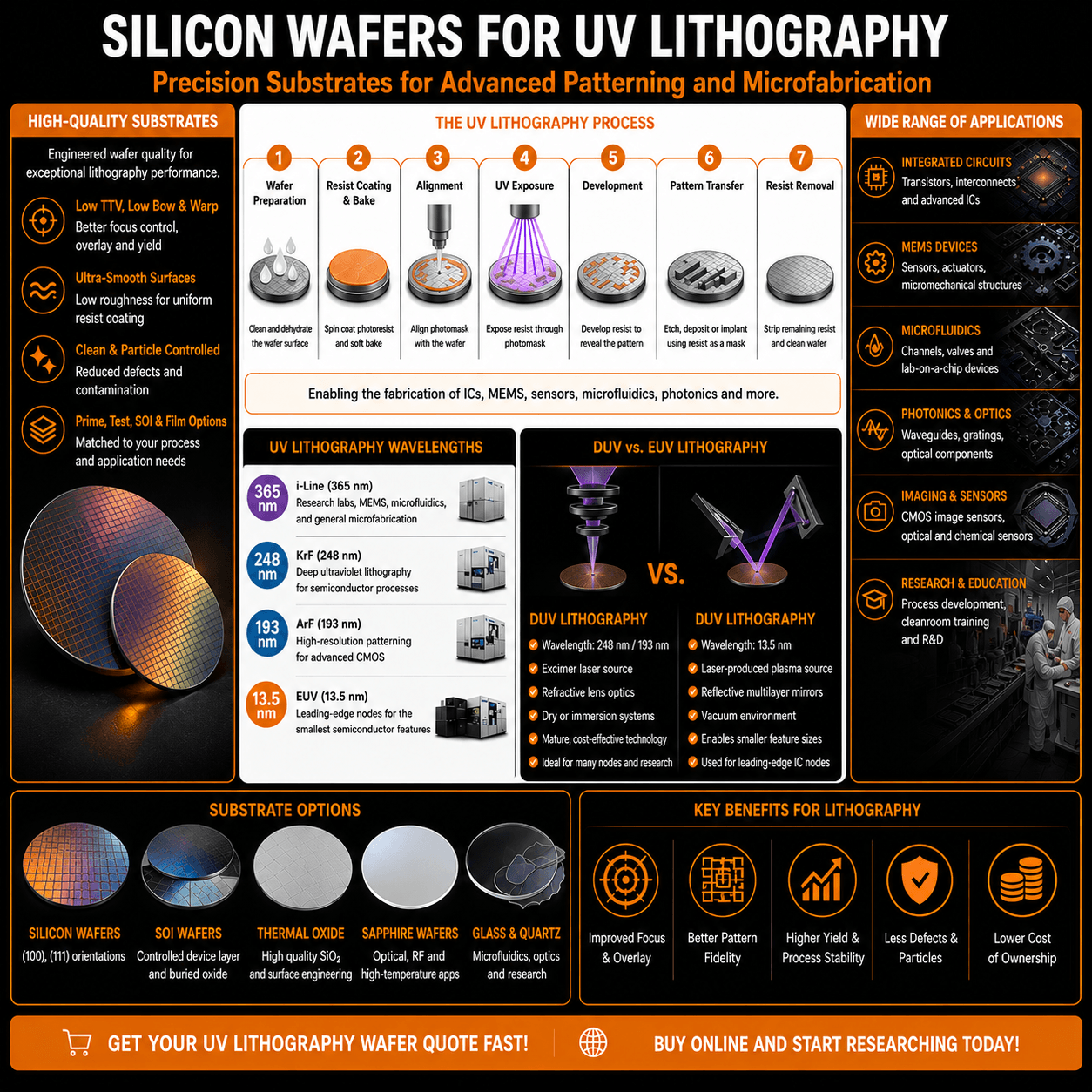
Photoresist is a photosensitive material whose solubility changes after exposure. The development behavior depends on the resist chemistry.
Resist thickness, exposure dose, bake conditions, development time, substrate reflectivity, and surface preparation can all influence the final lithographic profile and critical dimensions.
Shorter exposure wavelengths can support improved resolution, although actual feature size also depends on numerical aperture, imaging conditions, resist performance, process control, and patterning strategy.
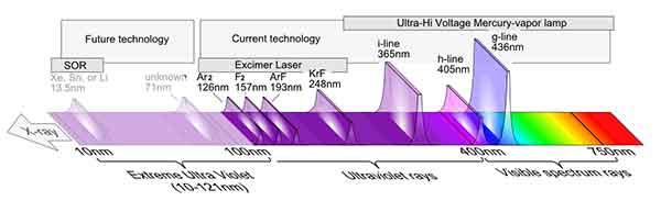
Modern lithography systems have progressed from 365 nm i-line exposure to 248 nm KrF and 193 nm ArF DUV technologies. EUV systems operate at a much shorter wavelength of 13.5 nm. :contentReference[oaicite:2]{index=2}
Deep ultraviolet (DUV) and extreme ultraviolet (EUV) are both used in advanced semiconductor patterning, but they use fundamentally different optical systems.
DUV lithography commonly uses 248 nm KrF or 193 nm ArF excimer-laser illumination. EUV lithography operates at 13.5 nm and requires reflective multilayer optics and a vacuum environment because EUV radiation is strongly absorbed by conventional transmissive optical materials and air. :contentReference[oaicite:3]{index=3}
| Feature | DUV Lithography | EUV Lithography |
|---|---|---|
| Common Wavelengths | 248 nm KrF and 193 nm ArF | 13.5 nm |
| Light Source | Excimer laser | Laser-produced plasma source in modern production tools |
| Projection Optics | Primarily refractive optical systems | Reflective multilayer mirrors |
| Operating Environment | Dry or immersion configurations depending on tool | Vacuum |
| Common Applications | Semiconductor manufacturing and advanced patterning | Leading-edge integrated circuit patterning |
| Resolution Strategy | Short wavelength, high numerical aperture, immersion and multiple patterning | Much shorter wavelength with advanced reflective optics |
| Major Challenge | Complex multiple-patterning schemes at the smallest pitches | Source, mask, optics, resist, contamination and tool complexity |
UV lithography is not limited to silicon. The exposure method can be applied to many substrates as long as the wafer or sample is compatible with the coating, exposure, alignment, handling, and downstream processing requirements.
Common substrate choices include:
Stanford's i-line photolithography facilities, for example, support silicon, silicon-germanium, quartz, sapphire, and glass substrates at 365 nm, demonstrating that UV lithography is used on a broader range of materials than silicon alone. :contentReference[oaicite:4]{index=4}
Substrate quality can influence photoresist coating, focus, alignment, overlay, defectivity, and pattern-transfer consistency. The most important wafer specifications depend on the exposure system and device process.
For many research applications, prime-grade silicon wafers provide excellent surface quality and flatness. Lower-cost test-grade wafers may be appropriate for process development when the required specifications allow them.
UV photolithography is used to fabricate a wide range of microscale and nanoscale devices and structures.
When selecting substrates for photolithography, researchers should provide the lithography tool and process requirements whenever possible.
Useful specifications include: