I need some low-quality n-type silicon doped GaAs wafers to 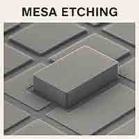 practice mesa etching. Any wafer is fine, as long as it's doped with n-Si so that electric measurements can be tested. About five wafers are needed.
Gallium Arsenide Wafers Used for Mesa Etching
A scientist asked for the following quote:
Reference #267786 for specs and pricing.
Get Your Quote FAST! Buy One Wafer Online! And Start Researching Today!
Quartz Wafers Used for Mesa Etching?
A researcher asked for us to qoute the following:
Do you supply Quartz? I was looking for some thin quartz, could I have some info and pricing on the quartz substrates you have?
Would you be able to tell me how easy it is to etch the quartz you supply? Would you be able to provide me with some info on the etchability of fused and crystalline quartz? We are looking for quartz with a very thin window layer say ~200nm on any of the thicker substrates? Could it be custom made?
Something like this, it would all be on the basis of controlled etching. Fig 1 shows an etched quartz window of ~200nm.
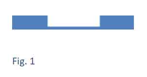
Etched Quartz Window
The other idea is to have a dielectric 200nm or so deposited and do a similar etch all the way upto glass (Fig 2) . Note in Fig 2 the dielectric should be a continuous layer across the sample.
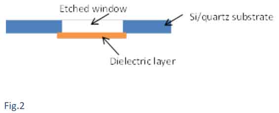
Etched Window, Si/Quartz Substrates, Dielectric Layer
We are very interested in a custom made structure. Specs are a bit tricky as we need to think about mechanical stability when we etch down to 200nm. We would like the window as large as possible (5mmx5mm at least). Yajie is the person working on the project, and I have cc’d her in. Please feel free to contact her for any additional info. Attached is a reference of similar structure on Si (see product DX-2513 and DX-2253). Our substrate can be either quartz or Si. SiN is preferable. Please feel free to contact one of us if you need more clarification. We would like this ASAP.
Could you let me know what the thickness of the thinnest quartz is? Also I am wondering if you have quartz windows of ultra thin layers?
UniversityWafer, Quoted:
a) Under the room temerture, the refractive of yellowish ray are n0=1.54422 and ne=1.55332 (the λof Na is 0.5893μm).
for fused quartz :Refractive index ( @ 589 nm ), Nd=1.4584
Reference #138234 for specs/pricing
What Is Mesa Etching?
If you're wondering what Mesa etching is, then this article is for you. It involves bevelling and undercutting,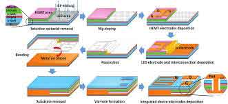 and removes superfluous metallization. As a result, this process reduces the chances of PR burning/erosion. In this article, we'll look at why this process is advantageous for some applications. Listed below are some benefits of Mesa etching.
Gas plasma etching is a well-known method for producing the mesa portion of a semiconductor device. The process was first described by Abe, Sonobe, and Enomoto in the Japan Journal of Applied Physics, Volume 12 No. 1 in 1973. Later, Devaney and Sheble described the process in Solid State Technology in December 1974. In the present article, we will discuss its advantages and disadvantages.
Wet etching in citric acid/peroxide was performed to define mesa structures. Two different chemical systems were used for the mesa etching. The chosen chemical system was based on the sidewall quality. Wet etching took approximately four minutes. The etching rate was not much different in the samples. The results are encouraging for the future development of high-density focal plane arrays.
In a Mesa etching process, a semiconductor wafer is exposed to an aqueous solution of NH4OH and H202. The solution contains a ratio of 14.5:3 - H202, and the concentration of NH4OH is 0.2 N. Once the process has completed, the semiconductor wafer is diced or broken. Mesa etching also removes the substrate material faster than the epitaxial layer material.
An optimized ICP etching recipe was developed for GaN SBD fabrication. A two-inch sapphire (0001) was etched with a GaN epi-layer. The n+-GaN conducting layer acted as a cathode electrode. The GaN epi-layer was etched to a depth of 10-8 A/cm2.
It involves undercutting and bevelling
The first electrolytic etching step provides the undercutting of portions 5 of the mesa. The second non-electrolytic etching step provides the bevel. This process is also effective in removing the masking pattern. The bevel extends upwardly about 0.2 microns from the top edge of the mesa. The mesa is then etched as described in the following sections.
Gas plasma etching is another technique for forming the mesa portion. This method avoids the inconvenience of wet chemical etching and allows for undercutting and bevelling without the use of a wet-chemical solution. Both processes are beneficial in different applications. Gas plasma etching is particularly useful in manufacturing semiconductor devices. It is also a good replacement for traditional wet chemical etching, which requires extra washing, drying, and cleaning steps.
For corners, the technique requires using a compensating structure. The compensation structure is a triangular shape, which has been shown in Figures 42(a) and 42(b). However, it is important to note that the etching solution used in the mesa process must be sufficient for the required etch depth. The compensating structure must be underetched completely. The compensation structure must be symmetrical to the mesa structure.
Chemical etching also uses a combination of nitric acid as oxidizer and hydrofluoric acid as a coordination agent. These chemicals are mixed with glacial acetic acid and acetone as solvent. The mixtures that were tested provided the best results. A number of experiments have been performed using chemical etching to produce complex shapes. It's worth mentioning that chemical etching does not involve the removal of the nitride layer.
It removes superfluous metallization
Mesa etching is a method for removing superfluous metallization from semiconductor wafers. During mesa etching, the semiconductor wafer is sliced between the mesa portions, and the etched areas are not connected to the contact portion 10. In the end, the mesa etching process removes the superfluous metallization from the substrate and allows the resulting device to be used.
Generally, the process involves two masking steps, the first one requiring an r.f. power of 50 watts, and the second step utilizing an oxygen-in-gas plasma. Both masking steps are essential for the final metallization, but they do not require high precision or accuracy. They are also suitable for fabricated redundant structures. Despite the complexity of the process, mesa etching is an effective method to remove superfluous metallization from semiconductor wafers.
In one aspect of the process, the upper edge of the mesa portion 5 is masked by a masking layer dot 4. This layer is used to protect the substrate from the electrolytic etchant. Another advantage of this method is that it removes the substrate material more quickly than the epitaxial layer material. For example, in a thin film process, the upper edge of the mesa portion is masked by the masking material. Once the top surface of the mesa portion has been exposed, the anode connection is made to it.
During the process, the active layer is made of 2 x 8 nm thick quantum wells. Then two AlAs layers are added for optical and electrical confinement. The whole process is schematically shown in Fig. 1. This process has been described earlier. Huffaker et al. used this process to remove the superfluous metallization from a silicon wafer.
It reduces PR burning/erosion issues
This technique can effectively etch mesa structures while minimizing the risk of damaging the GaN surface. In this study, ICP experiments were performed with a constant coil power of 500 W and a fixed total flow rate of 30 sccm. We found that higher plasma density and the production of higher Cl species led to better etching rates and improved surface morphology. We also evaluated the variations in the ion density with increasing pressure using Langmuir probe measurements and DECTAK-3 mechanical profiling.
A new dry etching process has been developed for mesa structures. This method has low pressure, low applied RF bias, and reduced microtrench issues. The technique also allows fabrication of GaN devices with a low-pressure and low-power photoresist mask. These results indicate that mesa etching can reduce the burning/erosion issues associated with PR.
A novel method for mesa etching that uses a mesa mask also reduces the risk of microtrench formation and increases mesa regrowth rates. For this procedure, we used a silicon dioxide hard mask and a photoresist hard mask. The negative photoresist was coated and developed in a krypton-based plasma to produce a mesa. After this, the mesa was hard baked in an oven and PR burning/erosion issues were reduced significantly.
It improves device uniformity
In the past few years, researchers have been working to improve the uniformity of CMOS devices. Several studies have demonstrated that mesa etching improves uniformity and minimizes device defects. This article will describe the basic concept behind mesa etching and present several experimental results. The first result is a comparison between the two mesa etching processes.
The mesa etching process uses hydrogen and methane to form the active area and base collector. The emitter metal acts as an etching mask. The mesa is formed by etching the material above the buried insulator layer 104. This step ensures that the active area 106 has a low epitaxial resistance and is not shorted by the base.
For this study, we examined a 4H-SiC wafer after the HF+NH4F treatment. The black dots represent the experimental profile; the blue and green lines represent the Gaussian components at 530.7 and 532.7 eV, respectively. A combined red line is the sum of these two lines. XPS atomic concentration analysis showed that the Si/C ratio is 1.0, thereby excluding carbon-rich sidewall surfaces.
For this research, engineers from Northrop Grumman have developed two gate formation refinements. These gate formation refinements have improved the uniformity of the etch process. The threshold voltage is uniform throughout the wafer, and a WIN gate with high device uniformity improves device performance. The etch stop process stops on an embedded layer in the barrier, resulting in excellent device uniformity. This process can improve device performance, but it also increases the process margin.
A mesa etching technique is capable of improving uniformity. The method can be applied to the fabrication of III-V devices, including Silicon Carbide (SiC) and Gallium Nitride. The authors collaborated with researchers at the University of Strathclyde and the University of California, Berkeley. Using a plasma and laser lift-off approach, these researchers have created a technique to fabricate GaN microcavities.
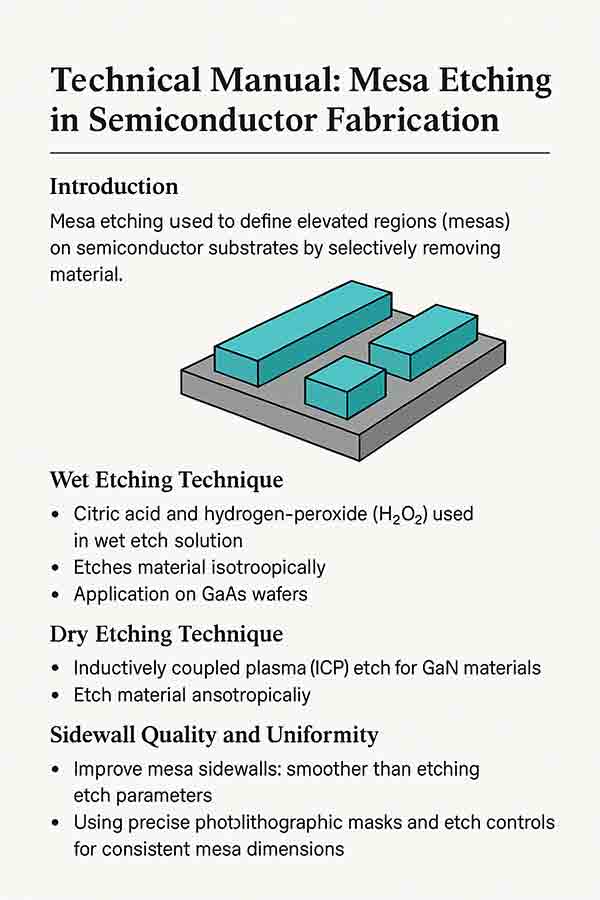
Technical Manual: Mesa Etching in Semiconductor Fabrication
Introduction
Mesa etching is used to define elevated regions (mesas) on semiconductor substrates by selectively removing material.
Wet Etching Technique
-
Citric acid and hydrogen peroxide (H₂O₂) used in wet etch solution
-
Etches material isotropically
-
Application on GaAs wafers
Dry Etching Technique
-
Inductively coupled plasma (ICP) etch for GaN materials
-
Etch material anisotropically
Sidewall Quality and Uniformity
-
Improve mesa sidewalls: smoother than etching etch parameters
-
Using precise photolithographic masks and etch controls for consistent mesa dimensions
