Based on the information of our project I will describe below, could you give me some suggestion about what specific type of wafer we need?
Basically, we need a 2-in Si wafer as the substrate. After basic cleaning process, we just want to simply deposit a layer of Silica Microsphere by spin-coating technique. No doped or any other IC fabrication will be involved. So I think the very basic Si wafer will satisfy our goal.
Please send me a list of wafer you recommend.
Deposit Layer of Silica Microsphere by Spin-Coating Technique
Silica Microsphere by Spin-Coating Technique
A PhD candidate needed us to recomend a sustrate sfor their research project.
Reference #126703 for specs and pricing.
Get Your Silicon Wafer Quote FAST! Or, Buy Online and Start Researching Today!
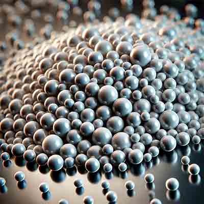
How are Microsphere Used In Semiconductors?
Microspheres play a significant role in the semiconductor industry, particularly in the manufacturing and processing of semiconductor devices. Here are some key applications:
-
CMP (Chemical Mechanical Planarization) Slurries:
- Planarization: Microspheres are used as abrasive particles in CMP
 slurries to achieve the planarization of semiconductor wafers. This process smooths the wafer surface by removing excess material and achieving a uniform, flat surface essential for subsequent photolithography steps.
 - Uniform Abrasion: The uniform size and shape of microspheres ensure consistent abrasion, reducing defects and improving the quality of the polished wafer.
- Planarization: Microspheres are used as abrasive particles in CMP
-
Wafer Cleaning:
- Particle Removal: Microspheres are employed in wafer cleaning processes to remove contaminant particles from the wafer surface. They help dislodge and carry away particles without causing damage to the delicate wafer surface.
- Non-abrasive Cleaning: For delicate cleaning tasks, non-abrasive microspheres are used to gently clean without scratching or damaging the wafer.
-
Packaging and Encapsulation:
- Encapsulation Materials: Microspheres can be part of the materials used for encapsulating semiconductor devices. They help improve the mechanical properties and reliability of the encapsulation materials, protecting the semiconductor devices from physical damage and environmental factors.
- Thermal Management: Certain microspheres, especially those made from materials with good thermal conductivity, are used in packaging materials to enhance heat dissipation from semiconductor devices.
-
Lithography:
- Resist Materials: Microspheres can be incorporated into photoresist materials used in photolithography processes. They help in defining fine patterns on the wafer by providing better control over the resist properties.
- Spacer Technology: In advanced lithography techniques, microspheres are used as spacers to maintain precise distances between different layers or components, ensuring accurate pattern transfer.
-
Advanced Applications:
- Nanotechnology: Microspheres are utilized in developing nanostructured materials and devices. They can serve as templates or building blocks for creating nanoscale features and patterns on semiconductor wafers.
- Optoelectronics: Microspheres with specific optical properties are used in the fabrication of optoelectronic devices, such as LEDs and photodetectors, enhancing their performance and efficiency.
Overall, microspheres contribute to various stages of semiconductor manufacturing, from wafer preparation and cleaning to lithography and packaging, ensuring high-quality and reliable semiconductor devices.
