
Could you please advise if the above type of silicon wafers will work for IR spectra under transmission mode too?
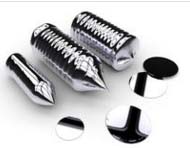
Semiconductor Grade Silicon
We provide the highest quality grade silicon for the semiconductor industry. Below is a recent quote from a PHD candidate out of a Texas University. You can purchase such wafers at our online store.
PHD Candidate
Wafers in Question:
100mm Undoped (100) 500um DSP FZ 10,000-20,000 ohm-cm
100mm Intrinsic (100) 500um DSP FZ >20,000 ohm-cm
Our reply:
Semiconductor grade Silicon has nil absorption in IR range 1.0 to 6.0µm. In the 6.0 to 25µm range there are several absorption bands. Furthermore Silicon has a rather large refractive index in this range so that in air reflections are significant (so that even with nil absorption the transmission is still only about 52%).
You need wafers polished on both sides (P/P or DSP), The smallest size that they normally come in is 2" diameter. Normally they are 0.3mm thick but we do have some that are 2mm thick and thicker.
Wafer resistivity >10 Ohmcm (whatever the dopant) is enough for Absorption to be nil in the 1.0 to 6.0µm range. However, the wafers marked FZ have nil Oxygen content, in contrast to wafers that are not so marked, which contain ~20ppma of dissolved Oxygen. That makes a difference in the vicinity of 7µm where there is a noticeable Oxygen Absorption band.
Crystallographic wafer orientation, [100] or [111] has no effect on IR optical properties of Silicon.
Get your quote FAST! Or, Buy Online and Start Researching Today!
What Specifications are Considered Electronic Grade Silicon?
Electronic Grade Silicon (EGS), also known as semiconductor-grade Silicon, is an ultra-pure form of Silicon that is used in the electronics and semiconductor industries to fabricate integrated circuits, solar cells, and other high-tech devices. This high purity level is crucial because even trace impurities can significantly affect the performance and efficiency of electronic devices.
Here are the key specifications of Electronic Grade Silicon:
- Purity: The most critical specification of EGS is its purity. Electronic Grade Silicon needs a purity level
 of 99.9999% (6N) or higher, with some applications requiring up to 99.9999999% (9N) purity. The higher the purity, the fewer impurities and defects, resulting in better device performance.
 - Dopant concentration: The concentration of intentional dopants like boron, phosphorus, arsenic, or antimony is tightly controlled to ensure precise electrical properties. The desired level of doping varies depending on the specific application.
- Trace impurities: The concentration of unintentional impurities, such as metals (e.g., aluminum, copper, iron), and other elements (e.g., carbon, oxygen) must be maintained at very low levels. These impurities can introduce defects and affect the electrical properties of the Silicon, leading to reduced device performance.
- Crystal structure: Electronic Grade Silicon is typically produced as monocrystalline or polycrystalline ingots. Monocrystalline Silicon is preferred for high-performance applications, as it has a more uniform crystal structure and fewer defects, resulting in better electrical properties. Polycrystalline Silicon, while less uniform, is more cost-effective and suitable for lower-performance applications like solar cells.
- Resistivity: The resistivity of Silicon is an important parameter in electronic devices, as it determines the electrical conductivity of the material. The resistivity of EGS is controlled by the concentration of dopants and the purity of the Silicon. Different applications require specific resistivity values, so ensuring that the EGS meets these requirements is essential.
- Surface finish and dimensions: The silicon ingots are often sliced into thin wafers for further processing. The surface finish of these wafers needs to be smooth and defect-free, as any imperfections can cause issues during the fabrication of electronic devices. Additionally, the wafers must be of uniform thickness and have well-defined dimensions to ensure proper device performance.
Electronic Grade Silicon is characterized by its high purity, controlled dopant concentrations, low trace impurity levels, well-defined crystal structure, specific resistivity, and precise surface finish and dimensions. These specifications ensure that the Silicon is suitable for the fabrication of high-performance electronic and semiconductor devices.
What is The Size & Growth of The Electronic Grade Silicon Market
The Electronic Grade Silicon Market has been segmented by types, applications, and players, offering detailed market data. The report includes comprehensive information on market drivers, growth opportunities, and emerging trends. It also provides in-depth analysis of key industry players. It examines the market for silicon and other materials in various end-use markets. The report offers the latest trends and technologies in the global semiconductor industry. It also offers in-depth knowledge about the various applications of semiconductors.
The U.S. Electronic Grade Silicon Market is the largest market in North America, accounting for 23% of the market's value sales volume. This region is expected to continue growing slowly over the coming years, thanks to the growing electronics and flat panel display industries. Saudi Arabia is also projected to experience strong revenue growth. However, the market for Semiconductor Grade Silicon is highly concentrated in Asia-Pacific, where the Chinese are the largest market.
The U.S. is the largest market for Electronic Grade Silicon, representing 23% of the overall market. Canada and Mexico are the next-largest markets, and are expected to grow gradually. The global market is expected to be driven by the growing flat-panel display industry and the growing semiconductor & electronics industries. The Saudi Arabian market is expected to grow at a healthy rate. Further, the booming solar cell industry is projected to boost the global market for Semiconductor Grade Silicon.
The market for Semiconductor Grade Silicon is primarily driven by the semiconductor and electronics industry. The semiconductor market is largely segmented by region, with the U.S. capturing 23% of the total value sales volume. But, as the semiconductor & electronics industry continues to expand, the market for Semiconductor Grade Silicon will expand gradually. The U.S. is also predicted to grow at a moderate rate in the near future due to the flat panel display industry and the increasing electronics and semiconductor industry. Meanwhile, the Saudi Arabian market is expected to grow at a good pace.
The global semiconductor grade silicon market is mainly driven by the demand for high-end smartphones and computer systems. The growing automotive industry and semiconductor & electronics industry are key end-use industries for this material. Further, the market is growing in Asia Pacific, Latin America, and the Middle East. For example, in the U.S., the largest market is in the U.S., followed by Mexico and Canada. This market is expected to grow slowly over the next few years.
The Electronic Grade Silicon market is segmented by type and application. The U.S. is the largest market in North America, with a 23% overall value sales volume share. Other countries in the region include the United Kingdom, China, Japan, Mexico, and Saudi Arabia. The U.S. is the largest electronic grade silicon market in the world, with a regional market of over $10 billion. The report covers the regional and global markets for Electronic Grade Silicon.
The Electronic Grade Silicon market is segmented by type and application. The U.S. leads the market with a 23% value sales volume share. Other countries include Mexico and Canada. While the U.S. is the largest country, it is expected to grow at a slow rate. The region's growing semiconductor & electronics industry is expected to drive growth in this region. Other countries such as Saudi Arabia are expected to see a strong growth in the market over the next few years.
The Electronic Grade Silicon market is categorized by type and application. The U.S. Electronic Grade Silicon market has a significant share of the North American market, with a 23% overall value sales volume. Other countries in the region include Canada and Mexico. The U.S. is expected to grow slowly over the next few years, driven by the growing electronics industry and flat panel display industry. The Gulf countries are also expected to show growth in the Electronic Grade Si market.
The Electronic Grade Silicon market is segmented by region. In the U.S., the Electronic Grade Silicon market has the highest value sales volume share in the region. In Canada, the Electronic Grade Si market is led by the U.S., and the next two countries are Mexico and Saudi Arabia. Further, the Asia-Pacific and Latin America markets are expected to grow at a moderate pace. Several countries in Asia and Africa are expected to witness the highest revenue growth in the future.
What is Semiconductor Grade Silicon?
The production of high-purity silicon for photovoltaics takes place in two stages. First, intermediate impurities of metallurgical silicon and semiconductor silicon are referred to as solar silicon. [Sources: 8]
Silica, a form of silicon (Sio 2), occurs naturally in the form of quartz. Silicon, besides oxygen, accounts for 27.8% of the earth's crust and is the most abundant element in nature. Unlike hydrogen and helium, which dominate visible matter in the universe, silicon has a mass content of less than 0.1%. [Sources: 2, 4, 8]
The use of silicon in semiconductor devices requires high-purity metallurgical silicon. The process of converting raw silicon into usable single crystal substrates in modern semiconductor processes begins with the degradation of pure silicon dioxide. Pure silicon (99.9%) is obtained by electrolysis from solid silicon and other silicon compounds. [Sources: 10, 12]
Known since 1854, this method has the potential to produce solar silicon without carbon dioxide emissions and with low energy consumption. The silicon itself does not conduct electricity, so it must be absorbed with doping agents to accurately control resistance. [Sources: 4, 12]
Moreover, the pure silicon used in integrated circuits consists of a single perfect crystal. A single silicon crystal consists of atoms in a three-dimensional periodic pattern that extends around the crystal. Semiconductors made of silicon become wafers that become silicon on the wafer. [Sources: 4, 11]
Polysilicon crystals, which form many smaller single crystals with different orientations, are not used in semiconductor devices. Czoralski's method is a method of crystal growth with which single crystal semiconductors can be produced. [Sources: 4, 7]
Electronic silicon (EGS) is the raw material for the production of single crystals made of silicon. Doping impurities (atoms such as boron and phosphorus) are added to high-purity semiconductor silicon (a few parts per million impurities) and the precise doping of the semiconductor turns it into P-type or ORN-type silicon, a type of silicon with different electronic properties. Semiconductor base materials are used to grow the crystals, and in the production of silicon wafers, the impurities are described as PbA and PbPma. [Sources: 7, 13]
Electronic silicon (EGS) is doped with elements in the range of parts per billion (ppb) carbon and less than 2 parts per million (ppm) - if silicon is purified by doping with elements such as boron, phosphorus and arsenic, it can be used as a semiconductor for various applications. Electronic silicon is a pure form of polycrystalline silicon that is converted into monocrystalline silicon ingots using the Czoralskis process. [Sources: 7]
Most of the Mg Si is used in metallurgical applications in silicon alloys such as aluminum and iron to improve certain properties. Polycrystalline poly is used to form component structures such as transistors, gates and integrated circuits. Electronic silicon and crystalline poly in amorphous (glass-like) non-crystalline form are used in photovoltaic (solar) cells and thin-film transistors. [Sources: 11]
Zone melting, also known as zone refining, was the first silicon cleaning method in which a bar of metallurgical silicon was heated to melt at one end. A heater moves the length of the rod and keeps a small length of it melted as it cools and solidifies. [Sources: 12]
The process of material removal removes the thin layer of silicon required for the production of wafers whose surfaces are free from damage. During this process, a haze can form on the surface of the wafer, giving it an additional polishing step to give it a mirrored finish. [Sources: 4]
TCs are evaporated and distilled until they reach a high degree of purity, then diluted with H2 before flowing into the deposition reactor, where they are converted into elementary silicon. This is naturally converted into Mg Si-TCs so that impurities such as Fe, Al and B can be removed. [Sources: 10]
The doping homogeneity in axial and radial directions is limited in Czochralski silicon, which makes it difficult to obtain wafers with a resistance of more than 100 ohms / cm. Silicon has a large refractive index (60-25 space) and a series of air reflections with significant (zero) absorption and transmission [52]. The oxygen and carbon impurities reduce the diffusion length of the silicon wafer. [Sources: 0, 5]
There is a strong need for theoretical and experimental analyses of the high-temperature capillarity phenomena and the moist propagation and infiltration that take place in selected Si-B and X-ceramic systems. In the following sections, we present an overview of the literature and data on theoretical and experimental studies of high-temperature phenomena occurring in the interaction of Si-based materials with available ceramics, as well as a summary of the conclusions of our research carried out using sessile drop-based methods in combination with various newly developed experimental methods. [Sources: 9]
A few refractory materials developed for high temperature photovoltaic silicon are dense graphite [34] (SIC), silicon graphite [5] and silicon nitride bled with silica [67], but these materials have not been widely used in LHTE systems due to varying operating conditions. [Sources: 9]
In addition, premium silicon wafers are expensive compared to other silicon grades, although their quality and extended life and performance justify the price. Pure silicon, also known as metallurgical silicon, is of good quality but unsuitable for the manufacture of electronic devices. The cost is prohibitive for other applications such as solar cells and liquid crystal displays (EGs), making upgraded surgical silicon (UMG-SI) an attractive alternative. [Sources: 1, 3]
Due to the high purity of quartz rock, beach sand and quartz are the most common raw materials for electronic grades. Not all sand is quartz, but sand extracted for this purpose has concentrations of quartz and silicon dioxide of up to 95%. Cleaning starts with heating the sand to reduce the carbon that carbon monoxide and silicon produce. [Sources: 8, 11]
On-line Tarre Filho, Artur Lange, Lisa C. Te, Celina de Melo, Gilberto Caldeira Bandeira Praes, Gustavo Eduardo 2016-02-01 Pyrolysis is the thermal degrading of organic materials by oxygen-free or lean oxygen in the atmosphere. Pyrolysis of chromium-rich tannins from industrial waste for the utilisation of carbonated waste in metallurgical processes. This study investigates the use of pyrolytic conversion of leather waste from chrome tanning processes into carbonated leather residues (CLR) for surgical CLR metal processing and the production of iron ore pellets. [Sources: 6]