
Why Is the Silicon Bohr Model Important?
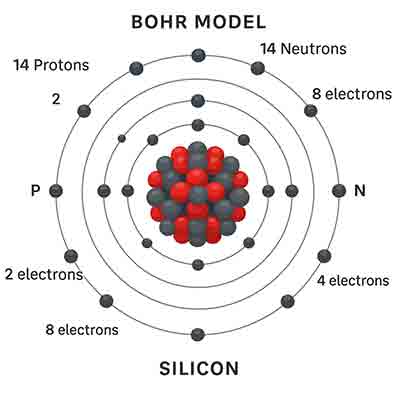
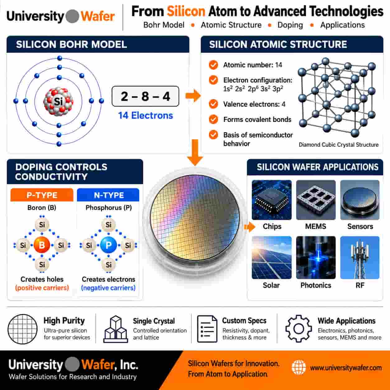
The Bohr model of silicon provides a simple way to visualize how the 14 electrons of a neutral silicon atom are distributed among electron shells. Silicon has a shell population of 2-8-4: two electrons in the first shell, eight in the second, and four in the outermost shell.
Those four valence electrons are especially important because they participate in chemical bonding and help explain how silicon atoms form the crystalline structures used in silicon wafers. Understanding this simplified atomic model provides a useful starting point for studying covalent bonding, semiconductor band structure, doping, charge carriers, and electronic devices.
The Bohr model should not be interpreted as a literal picture of electrons traveling in fixed circular paths. Modern quantum mechanics describes electrons using orbitals and probability distributions. The ground-state electron configuration of silicon is 1s² 2s² 2p⁶ 3s² 3p², while 2-8-4 is a convenient way to describe the number of electrons associated with each principal shell.
Silicon Wafers for Semiconductor Research
Understanding the silicon Bohr model is only the beginning. Researchers can apply these atomic and semiconductor concepts using real silicon substrates for experiments involving doping, oxidation, lithography, thin-film deposition, etching, MEMS, sensors, photovoltaics, and electronic-device fabrication.
Get Your Silicon Wafer Quote FAST! Or Buy Silicon Wafers Online and start researching today.
From a Silicon Atom to a Silicon Crystal
A semiconductor wafer does not consist of isolated silicon atoms. In single-crystal silicon, atoms are arranged in a repeating diamond-cubic crystal structure. Each silicon atom is tetrahedrally coordinated to four nearest-neighbor silicon atoms through covalent bonding.
This ordered atomic arrangement gives crystalline silicon properties that are essential to semiconductor technology. Silicon wafers can be produced with carefully controlled crystal orientation, dopant concentration, resistivity, thickness, and surface finish for different fabrication processes and device architectures.
Researchers can learn more about the dimensions of this crystalline structure in our guide to the silicon lattice constant.
How Atomic Structure Leads to Semiconductor Behavior
The Bohr model is useful for introducing valence electrons, but semiconductor behavior is more accurately explained using energy-band theory. When a large number of silicon atoms form a crystal, their allowed electronic states form energy bands rather than remaining as the discrete energy levels of isolated atoms.
In crystalline silicon, the valence band and conduction band are separated by an indirect energy band gap of approximately 1.12 eV at room temperature. Electrons that acquire sufficient energy can be excited into the conduction band, leaving holes in the valence band. Both electrons and holes can contribute to electrical conduction.
Learn more about this relationship in our guide to the silicon band gap.
Why Silicon Has Four Valence Electrons
Silicon has atomic number 14 and is located in Group 14 of the periodic table. Its outer-shell configuration is 3s²3p², giving a neutral silicon atom four valence electrons.
In crystalline silicon, bonding involves these valence states and produces the tetrahedral bonding network characteristic of the diamond-cubic lattice. This provides a useful connection between the simple Bohr representation and the more complete description of crystalline silicon used in materials science and semiconductor physics.
See where Si appears among the elements in our Silicon on the Periodic Table guide.
How Doping Changes Silicon's Electrical Properties
Pure crystalline silicon is an intrinsic semiconductor, but most electronic devices require carefully controlled electrical properties. These properties can be modified by introducing small, controlled concentrations of impurity atoms known as dopants.
P-Type Silicon
Group 13 elements such as boron have three valence electrons and can act as acceptor dopants when incorporated substitutionally into silicon. Acceptor doping increases the concentration of holes, producing p-type silicon.
N-Type Silicon
Group 15 elements such as phosphorus and arsenic have five valence electrons and can act as donor dopants in silicon. Donor doping increases the concentration of conduction electrons, producing n-type silicon.
Controlling dopant species and concentration allows wafer manufacturers and device engineers to tailor properties such as carrier concentration and electrical resistivity. Explore the different approaches in our silicon wafer doping techniques guide.
From P-Type and N-Type Silicon to Semiconductor Devices
Controlled p-type and n-type regions are fundamental building blocks of semiconductor technology. By engineering these regions within silicon, researchers can create p-n junctions and more complex structures used in diodes, transistors, integrated circuits, photodetectors, solar cells, and many other electronic and optoelectronic devices.
Modern devices depend on much more than the simple atomic picture shown by the Bohr model, but the model provides an intuitive introduction to why valence electrons and dopant atoms matter when engineering the electrical properties of silicon.
Why Silicon Is Used for Semiconductor Wafers
Silicon's importance to semiconductor manufacturing comes from a combination of material and processing advantages. High-purity silicon can be grown as large single crystals, its electrical properties can be controlled through doping, and it forms a high-quality silicon dioxide layer that is extremely useful in semiconductor processing.
Silicon dioxide (SiO2) can serve as an insulating dielectric, surface-passivation layer, diffusion or implantation mask, and processing layer in many device-fabrication sequences.
These characteristics, combined with decades of highly developed manufacturing infrastructure, make silicon an important substrate for:
- Integrated circuits – processors, memory, logic, and analog devices
- MEMS – sensors, resonators, accelerometers, and microactuators
- Photovoltaics – crystalline-silicon solar cells
- Power electronics – diodes, MOSFETs, IGBTs, and related devices
- Sensors – pressure, temperature, optical, chemical, and other sensing structures
- Photonics – silicon photonic structures and integrated optical devices
- Research and education – semiconductor physics, materials science, chemistry, and microfabrication experiments
Choosing Silicon Wafers for Research
Researchers applying these concepts in the laboratory should consider several specifications when selecting a silicon substrate. Common requirements include:
- Wafer diameter
- Crystal orientation such as (100), (110), or (111)
- Conductivity type – p-type or n-type
- Dopant species
- Resistivity range
- Wafer thickness
- Single-side or double-side polish
- Crystal growth method
These parameters can affect electrical measurements, oxidation, etching, thin-film processing, MEMS fabrication, and device performance. UniversityWafer supplies silicon substrates in a range of specifications for universities, laboratories, semiconductor development, and industrial research.
Silicon Bohr Model at a Glance
Silicon (Si) has atomic number 14, meaning every silicon atom contains 14 protons. A neutral silicon atom also contains 14 electrons. In the simplified Bohr model, those electrons are distributed among three occupied shells in a 2–8–4 configuration.
| Atomic Property | Silicon (Si) |
|---|---|
| Atomic Number | 14 |
| Periodic Table Group | 14 (Carbon Group) |
| Period | 3 |
| Occupied Electron Shells | 3 |
| Electrons by Shell | 2–8–4 |
| Valence Electrons | 4 |
| Ground-State Electron Configuration | 1s² 2s² 2p⁶ 3s² 3p² |
| Crystal Structure | Diamond cubic |
| Band Gap Near Room Temperature | Approximately 1.12 eV (indirect) |
What the 2–8–4 Silicon Electron Configuration Means
The 2–8–4 shell notation is a simplified way of describing the distribution of silicon's 14 electrons. The first two shells contain 2 and 8 electrons, while the third occupied shell contains four valence electrons.
In the more complete quantum-mechanical description, silicon has the ground-state electron configuration 1s² 2s² 2p⁶ 3s² 3p². The four electrons in the 3s and 3p valence states participate in chemical bonding.
This distinction is important: the Bohr model is an educational representation, while orbital theory and quantum mechanics provide the more accurate description required for semiconductor physics.
Silicon Valence Electrons and Crystal Bonding
In crystalline silicon, each atom is tetrahedrally coordinated to four nearest-neighbor silicon atoms. The resulting covalent-bond network forms the diamond-cubic crystal structure characteristic of single-crystal silicon.
Semiconductor wafers are cut from these single crystals along specific crystallographic planes. Common wafer orientations include (100), (110), and (111).
Crystal orientation matters because it can influence surface structure, oxidation, carrier transport, mechanical behavior, and orientation-dependent etching. Learn more about silicon wafer orientation and the silicon crystal lattice.
From Atomic Energy Levels to Silicon Energy Bands
The Bohr model describes energy levels for an individual atom, but a silicon wafer contains an enormous number of atoms arranged in a crystal. When these atoms interact, their allowed electronic states form energy bands.
Two bands are especially important in semiconductor physics:
- Valence band – the highest range of occupied states at absolute zero, associated with the bonding states of the silicon crystal.
- Conduction band – higher-energy allowed states in which electrons can contribute to electrical conduction.
These bands are separated by an energy range with no allowed bulk electronic states called the band gap. Crystalline silicon has an indirect band gap of approximately 1.12 eV near room temperature.
Electrons, Holes and Electrical Conduction
When sufficient energy is supplied to crystalline silicon, an electron can be excited from the valence band into the conduction band. This leaves an unoccupied electronic state in the valence band that behaves as a positive charge carrier called a hole.
Electrons in the conduction band and holes in the valence band can both contribute to electrical current. Their concentrations and transport properties are central to the operation of semiconductor devices.
In intrinsic silicon, electron-hole pairs can be generated thermally or optically. In doped silicon, donor or acceptor impurities provide additional carriers and allow engineers to control the electrical properties much more precisely.
How Doping Changes a Silicon Wafer
Semiconductor manufacturers intentionally introduce selected impurity atoms into silicon to modify carrier concentration and electrical resistivity. This process is known as semiconductor doping.
| Dopant | Periodic Group | Role in Silicon | Conductivity Type |
|---|---|---|---|
| Boron (B) | Group 13 | Acceptor | P-Type |
| Phosphorus (P) | Group 15 | Donor | N-Type |
| Arsenic (As) | Group 15 | Donor | N-Type |
| Antimony (Sb) | Group 15 | Donor | N-Type |
Dopant concentration can span many orders of magnitude depending on the intended application. As a result, simply specifying "p-type" or "n-type" is often not enough when selecting a wafer; researchers should also specify the required resistivity or dopant concentration range.
UniversityWafer supplies p-type silicon and n-type silicon in a range of resistivities, orientations, thicknesses, and surface finishes.
How Silicon Atomic Properties Affect Wafer Applications
Silicon's usefulness as a substrate results from much more than having four valence electrons. Its semiconductor band structure, controllable doping, crystalline quality, mechanical properties, and compatibility with mature fabrication processes make it suitable for a broad range of electronic and microsystem technologies.
| Silicon Property | Why It Matters | Example Applications |
|---|---|---|
| Controllable Doping | Allows carrier concentration and resistivity to be engineered | Diodes, transistors, integrated circuits |
| High-Quality SiO₂ | Provides useful dielectric, passivation, and processing layers | MOS devices, IC fabrication, sensors |
| Single-Crystal Structure | Provides controlled electrical and mechanical properties | ICs, MEMS, research devices |
| Orientation-Dependent Properties | Enables process and device optimization | MEMS, anisotropic etching, microfabrication |
| Semiconductor Band Structure | Enables controlled electron and hole transport | Electronics, sensors, photovoltaics |
Silicon Wafer Applications
The atomic and electronic properties introduced by the silicon Bohr model ultimately connect to real substrate applications. Silicon wafers are used as starting materials for:
- Integrated circuits – logic, memory, processors, and analog electronics
- MEMS – accelerometers, pressure sensors, microphones, resonators, and actuators
- Photovoltaics – crystalline-silicon solar cells and photovoltaic research
- Photonics – waveguides, modulators, detectors, and integrated photonic structures
- Power devices – silicon MOSFETs, IGBTs, diodes, and related structures
- Sensors – optical, chemical, mechanical, and electrical sensing devices
- Microfabrication research – lithography, etching, oxidation, deposition, and device prototyping
From Silicon Crystal to Finished Wafer
Semiconductor-grade silicon is purified and grown into single-crystal ingots using methods such as the Czochralski process or Float Zone crystal growth.
The crystal is then oriented, shaped, sliced, edge-finished, lapped or ground as required, chemically etched, polished, and cleaned to produce wafers suitable for semiconductor processing.
Depending on the application, silicon wafers may subsequently undergo thermal oxidation, diffusion, ion implantation, photolithography, wet or dry etching, thin-film deposition, epitaxy, metallization, wafer bonding, thinning, and dicing.
These processes transform the highly ordered silicon crystal into the patterned structures required for modern semiconductor and MEMS devices.
Choosing the Right Silicon Substrate
Researchers ordering silicon wafers should select specifications based on the intended device and fabrication process rather than atomic structure alone. Important parameters include:
- Diameter – wafer size required by the process equipment
- Crystal orientation – commonly (100), (110), or (111)
- Conductivity type – p-type or n-type
- Dopant – such as boron, phosphorus, arsenic, or antimony
- Resistivity – selected for the required electrical behavior
- Thickness – standard or custom substrate thickness
- Surface finish – single-side polished or double-side polished
- Growth method – Czochralski or Float Zone when relevant
Connecting these wafer specifications to silicon's atomic, crystalline, and electronic properties helps researchers select substrates appropriate for semiconductor fabrication, materials science, MEMS, photonics, photovoltaics, and device development.
Silicon Bohr Model FAQs
What is the Bohr shell configuration of silicon?
Silicon has a simplified Bohr shell configuration of 2–8–4: two electrons associated with the first shell, eight with the second, and four with the third.
How many valence electrons does silicon have?
A neutral silicon atom has four valence electrons. Its ground-state outer electron configuration is 3s²3p².
How many protons and electrons does silicon have?
Silicon has atomic number 14, so every silicon atom contains 14 protons. A neutral silicon atom also contains 14 electrons.
Does silicon always have 14 neutrons?
No. The number of neutrons depends on the isotope. Silicon-28, the most abundant stable isotope, has 14 neutrons, while other silicon isotopes contain different numbers of neutrons.
Is the Bohr model an accurate picture of a silicon atom?
It is a useful simplified model, but it is not a literal representation of electron motion. Quantum mechanics describes electrons using orbitals and probability distributions rather than fixed circular paths around the nucleus.
Related Silicon and Semiconductor Resources
- Silicon Atomic Structure – Learn about silicon atoms, electron configuration, protons, neutrons, isotopes, and atomic bonding.
- Silicon on the Periodic Table – Explore silicon as element 14, including its Group 14 position, electron configuration, and semiconductor properties.
- What Is Silicon? – Learn about silicon properties, crystal structure, semiconductor behavior, and wafer applications.
- Silicon Wafers – Explore silicon substrates by diameter, crystal orientation, resistivity, dopant type, thickness, and surface finish.
- Silicon Band Gap – Learn how silicon's valence and conduction bands relate to electron-hole generation and semiconductor behavior.
- Silicon Lattice Constant – Explore the diamond-cubic crystal structure and lattice dimensions of crystalline silicon.
- Silicon Wafer Doping Techniques – Compare techniques used to introduce donor and acceptor dopants and control silicon electrical properties.
- P-Type Silicon – Learn how acceptor dopants such as boron increase hole concentration in silicon.
- N-Type Silicon – Learn how donor dopants such as phosphorus and arsenic increase electron concentration in silicon.
- Thermal Oxide on Silicon – Learn how SiO2 layers are formed on silicon and used in semiconductor processing.
- Silicon Wafer Applications – See how silicon substrates are used for integrated circuits, MEMS, sensors, photovoltaics, photonics, and research.