Silicon Carbide (SiC) Substrate for Research & Production
Silicon carbide wafers, also known as SiC substrates, provide the wide bandgap, high thermal conductivity, and high breakdown strength required for power electronics, electric vehicle inverters, RF devices, aerospace systems, and high-temperature semiconductor research. UniversityWafer supplies 4H-SiC and 6H-SiC wafers in N-type and semi-insulating grades, with on-axis or off-axis orientations, custom thicknesses, diced samples, and epi-ready CMP surfaces for device fabrication, epitaxial growth, and materials research.
Request 4H-SiC and 6H-SiC Wafers
UniversityWafer, Inc. supplies 4H-SiC and 6H-SiC wafers for power electronics, epitaxial growth, RF devices, materials science, high-temperature sensors, and semiconductor research. Available options may include N-type silicon carbide, semi-insulating SiC, on-axis and off-axis orientations, single-side or double-side polishing, and epi-ready CMP surfaces.
Researchers may request full SiC wafers, diced chips, custom-cut samples, test-grade material, or
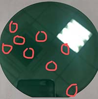
broken SiC substrates
for budget-conscious experiments.
Research Request for Multiple SiC Wafer Sizes
A university researcher requested pricing and specifications for the following:
We are interested in purchasing silicon carbide wafers and would like information about wafer thickness, SiC polytype, crystal orientation, surface finish, and pricing.
2-inch SiC wafers
3-inch SiC wafers
4-inch SiC wafers
6-inch SiC wafers
We would initially like to test several lower-cost or broken wafers to determine whether the damaged areas affect our research. If they work for our application, we may purchase additional quantities.
Refer to Request #247746 when asking about similar 4H-SiC or 6H-SiC specifications.
Broken, chipped, reclaimed, and lower-grade silicon carbide substrates can provide an affordable alternative for experiments that do not require an intact prime wafer. UniversityWafer helps budget-conscious university laboratories locate SiC pieces suitable for cleaving, deposition trials, microscopy, process development, and preliminary material testing.
As a university laboratory with a limited budget, we would like to test several broken SiC wafers before purchasing a larger quantity. Please include the thickness, 4H or 6H polytype, crystal orientation, and surface condition with the quote.
Example SiC Wafers Quoted
Four 2-inch 4H-SiC wafers:
approximately 350 µm thick, <0001> on-axis orientation
One 3-inch 4H-SiC wafer:
approximately 350 µm thick, <0001> orientation with a 4° off-axis angle
Diced 4H-SiC and 6H-SiC Samples
Small SiC chips and diced substrates may be available for researchers who do not require a full wafer. Common research sizes may include:
5 × 5 mm SiC chips
6 × 6 mm SiC chips
10 × 10 mm SiC chips
2-inch SiC wafers
Custom-cut silicon carbide pieces
Available material may include 4H-SiC and 6H-SiC with N-type conductivity, single-side polishing, and resistivity ranges suitable for materials and semiconductor research. Inventory changes, so researchers should submit acceptable specification ranges rather than relying on one exact item.
Geometry: Bow, warp, and TTV specifications available by grade
Surface: Double-side polished with an epi-ready Si-face CMP surface
Surface roughness: Less than approximately 0.5 nm
3-Inch Semi-Insulating 4H-SiC
Polytype: 4H-SiC
Electrical type: Semi-insulating
Orientation: <0001> ±0.5°
Thickness: 350 ±25 µm
Resistivity: High-resistivity specifications available by grade
Surface: Double-side polished with an epi-ready Si-face CMP surface
Typical use: RF, microwave, GaN-on-SiC, and electrically isolated structures
2-Inch Semi-Insulating 6H-SiC
Polytype: 6H-SiC
Electrical type: Semi-insulating
Orientation: <0001> ±0.5°
Thickness: 330 ±25 µm
Resistivity: High-resistivity specifications available by grade
Surface: Single-side polished with an epi-ready Si-face CMP surface
4-Inch 4H-SiC, N-Type
Diameter: 100 mm ±0.38 mm
Polytype: 4H-SiC
Conductivity: N-type, nitrogen doped
Orientation: 4.0° ±0.5° off-axis
Thickness: 350 ±25 µm
Resistivity: Approximately 0.01–0.1 Ω·cm
Surface: Double-side polished with an epi-ready Si-face CMP surface
Surface roughness: Less than approximately 0.5 nm
These specifications are examples of previously available research material and should not be interpreted as guaranteed current inventory. Submit your acceptable polytype, diameter, orientation, thickness, resistivity, grade, and quantity so UniversityWafer can identify the closest available substrate.
Broken Silicon Carbide for Cleaving Experiments
Broken SiC wafers may be especially useful as cleaving substrates. Researchers can cut or cleave smaller pieces from the undamaged portions, reducing material costs when a full-diameter prime wafer is unnecessary.
The broken 2-inch SiC wafers we previously purchased worked well as cleaving substrates. We are now interested in several thicker 3-inch or 4-inch 4H-SiC wafers and would like information about quantity discounts.
3-inch broken 4H-SiC, approximately 500 or 700 µm thick, <0001> orientation, 4° off-axis
4-inch broken 4H-SiC, approximately 500 µm thick, <0001> on-axis or 4° off-axis
How to Request a SiC Substrate
Include as many of the following specifications as possible:
4H-SiC or 6H-SiC polytype
Full wafer, broken wafer, or diced chip
Wafer diameter or sample dimensions
On-axis or off-axis orientation
N-type or semi-insulating material
Required resistivity range
Wafer thickness
Si-face or C-face surface
SSP, DSP, or epi-ready CMP finish
Surface roughness requirement
Bow, warp, and TTV limits
Research, test, production, B-grade, or D-grade material
Quantity and target budget
Silicon Carbide Wafers for Power Electronics and Semiconductor Research
UniversityWafer, Inc. supplies
silicon carbide wafers
for power electronics, electric vehicles, RF devices, high-temperature sensors, renewable-energy systems, and advanced semiconductor research. Available materials include 4H-SiC and 6H-SiC substrates with N-type, semi-insulating, on-axis, and off-axis specifications.
Compared with conventional
silicon wafers,
SiC substrates provide a wider bandgap, higher critical electric field, strong thermal conductivity, high-temperature capability, and excellent resistance to harsh operating conditions. These material properties make silicon carbide especially useful for devices that must control high voltage and current while minimizing power loss.
Common Silicon Carbide Wafer Applications
Electric vehicle traction inverters
Onboard chargers and DC-DC converters
Fast-charging infrastructure
Solar and wind power converters
Industrial motor drives
High-voltage power supplies
RF and microwave electronics
Radar and wireless communication systems
Aerospace and satellite electronics
High-temperature sensors
Harsh-environment semiconductor devices
SiC epitaxy and power-device research
Why Silicon Carbide Is a Wide-Bandgap Semiconductor
Silicon carbide is classified as a
wide-bandgap semiconductor.
The bandgap varies by polytype, with 4H-SiC commonly cited at approximately 3.26 eV and 6H-SiC at approximately 3.0 eV. By comparison, silicon has a bandgap of approximately 1.12 eV at room temperature.
A wider bandgap helps SiC semiconductor devices maintain useful electrical performance at higher temperatures and withstand stronger electric fields before breakdown. This allows manufacturers to design smaller, faster, and more efficient power devices for high-voltage applications.
The larger bandgap does not mean that SiC stores energy like a battery. Instead, it describes the energy required for electrons to move from the valence band to the conduction band. This electronic property contributes to the material's ability to support high-temperature and high-voltage semiconductor operation.
Advantages of Silicon Carbide Over Silicon
Silicon remains the dominant semiconductor material for integrated circuits and many low- to medium-voltage devices. However, SiC offers important performance advantages in demanding power-electronics applications.
Higher breakdown field:
SiC can support stronger electric fields, enabling thinner drift layers and higher-voltage devices.
Lower power losses:
Properly designed SiC MOSFETs and diodes can reduce conduction and switching losses in power-conversion systems.
Higher operating temperature:
SiC devices can function in environments where conventional silicon electronics may require more intensive cooling.
High thermal conductivity:
Efficient heat transfer can simplify thermal management and improve power density.
Higher switching frequency:
Faster switching can allow smaller inductors, transformers, capacitors, and cooling components.
Radiation and environmental resistance:
SiC is studied for aerospace, nuclear, and other harsh-environment applications.
Silicon Carbide for Electric Vehicle Power Electronics
Silicon carbide is used in electric vehicles primarily in power-conversion electronics, not as the battery's energy-storage material. SiC MOSFETs and Schottky barrier diodes can be incorporated into traction inverters, onboard chargers, DC-DC converters, and fast-charging systems.
In a traction inverter, power semiconductor devices convert direct current from the battery into alternating current for the electric motor. Reducing switching and conduction losses can improve system efficiency, decrease heat generation, and reduce the size of cooling components.
Potential advantages of SiC electric vehicle electronics include:
Improved inverter efficiency
Higher-voltage power architectures
Reduced cooling requirements
Smaller and lighter power modules
Higher switching frequencies
Faster onboard and external charging
Greater power density
Potential improvements in driving range
The actual benefit depends on the device design, voltage platform, drive cycle, packaging, thermal management, and overall vehicle architecture. Silicon carbide components can cost more to manufacture than comparable silicon devices, but their system-level efficiency may offset part of the initial expense.
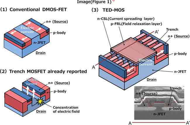
The high critical electric field of silicon carbide makes it well suited for power devices that control hundreds or thousands of volts. SiC substrates are used in the development of MOSFETs, Schottky barrier diodes, junction barrier Schottky diodes, and other discrete power components.
These devices are used in applications where electrical efficiency, high power density, and reliable operation are important, including:
Electric and hybrid-electric vehicles
Rail transportation
Aircraft power systems
Photovoltaic inverters
Wind-turbine converters
Industrial power supplies
Motor drives and robotics
Data-center power conversion
Smart-grid equipment
Silicon Carbide for RF and Microwave Devices
Semi-insulating silicon carbide provides high electrical resistivity and strong thermal conductivity, making it an important substrate for RF and microwave research. It can support epitaxial materials and device structures used in radar, telecommunications, satellite communication, and high-frequency power amplifiers.
Common RF research applications include:
GaN-on-SiC high-electron-mobility transistors
Radar transmit-and-receive modules
Microwave power amplifiers
Wireless base-station electronics
Satellite communication systems
High-frequency semiconductor testing
Researchers studying RF devices often request semi-insulating 4H-SiC wafers because their high resistivity helps reduce parasitic conduction while their thermal properties support heat dissipation.
4H-SiC vs. 6H-SiC Wafers
Silicon carbide can form many crystal structures known as polytypes. The two most commonly requested research polytypes are 4H-SiC and 6H-SiC.
Property
4H-SiC
6H-SiC
Crystal structure
Hexagonal
Hexagonal
Approximate bandgap
3.26 eV
Approximately 3.0 eV
Common conductivity options
N-type and semi-insulating
N-type and semi-insulating
Typical research uses
Power devices, SiC epitaxy, MOSFETs, diodes, and RF structures
Materials research, optical experiments, sensors, and legacy device studies
Common orientation
On-axis or off-axis from <0001>
Generally on-axis or near <0001>
4H-SiC is generally preferred for modern power-electronics research because of its favorable carrier mobility and high critical electric field. 6H-SiC remains useful for materials science, optical, sensor, and specialized semiconductor experiments.
N-Type and Semi-Insulating SiC Substrates
The electrical specification of a SiC wafer should be selected according to the intended device or experiment.
N-type SiC:
Commonly nitrogen-doped and used for conductive substrates, epitaxial growth, power devices, diodes, and MOSFET development.
Semi-insulating SiC:
Designed for very high resistivity and frequently used for RF, microwave, GaN-on-SiC, and electrically isolated device structures.
Important ordering specifications include polytype, conductivity type, resistivity, diameter, thickness, crystal orientation, off-axis angle, surface finish, micropipe density, total thickness variation, bow, warp, and defect requirements.
Silicon carbide substrates are available for power-device, RF, epitaxial-growth, and high-temperature semiconductor research.
On-Axis and Off-Axis SiC Wafers
SiC wafers may be supplied on-axis or with the surface intentionally cut several degrees away from the primary crystal plane. Off-axis 4H-SiC wafers, including common 4-degree specifications, are widely used for homoepitaxial SiC growth because the miscut promotes controlled step-flow growth.
On-axis SiC: Used for selected research, optical, sensor, and specialized growth applications.
Off-axis SiC: Frequently selected for epitaxial layers used in power-device fabrication.
The correct orientation depends on the deposition method, device structure, epitaxial process, and research objective.
Epi-Ready Silicon Carbide Surfaces
An epi-ready SiC wafer typically receives precision polishing and
chemical mechanical polishing (CMP)
to produce a smooth surface suitable for epitaxial growth. Surface quality is important because polishing damage, scratches, particles, and subsurface defects can influence the quality of deposited semiconductor layers.
Researchers may request:
Silicon-face or carbon-face polishing
Single-side polished SiC wafers
Double-side polished SiC wafers
Epi-ready CMP surfaces
Research-grade or production-grade substrates
Custom surface roughness specifications
Diced SiC chips or custom-cut samples
Silicon Carbide in Renewable Energy Systems
SiC power devices can increase the efficiency and power density of converters used in solar, wind, battery-storage, and smart-grid systems. Higher switching frequencies may allow designers to reduce the size of passive components, while lower losses can reduce cooling requirements.
Renewable-energy applications include:
Photovoltaic string and central inverters
Wind-turbine power converters
Battery energy-storage systems
High-voltage DC transmission research
Grid-connected power supplies
Industrial energy-conversion systems
Silicon Carbide for Aerospace and Harsh Environments
Silicon carbide is studied for electronics and sensors that operate under high temperature, radiation, mechanical stress, and corrosive conditions. Potential applications include spacecraft power systems, satellite communication, turbine monitoring, combustion sensing, nuclear instrumentation, and high-temperature industrial controls.
SiC does not make every electronic component inherently radiation-proof. Device architecture, dielectric quality, packaging, dose, particle type, and operating conditions all influence radiation performance. However, its material properties make it a valuable platform for radiation-tolerant and harsh-environment semiconductor research.
Advantages and Limitations of SiC Substrates
Advantages
Wide bandgap
High critical electric field
Strong thermal conductivity
High-temperature operation
High-frequency switching capability
Low power-conversion losses
High power density
Resistance to harsh environments
Compatibility with SiC epitaxial device layers
Limitations
Higher substrate and fabrication costs than conventional silicon
Difficult crystal growth and wafer processing
Material defects that can affect device yield
Specialized implantation, annealing, etching, and contact processes
More demanding surface preparation and epitaxial growth
Smaller manufacturing ecosystem than mature silicon technology
These limitations do not make SiC unsuitable for semiconductor manufacturing. Instead, they explain why substrate quality, process control, defect inspection, and appropriate wafer specifications are especially important.
How to Specify a Silicon Carbide Wafer
Include the following information when requesting a SiC wafer quote:
Polytype: 4H-SiC or 6H-SiC
Diameter: Full wafer, small wafer, diced chip, or custom piece
Conductivity: N-type or semi-insulating
Dopant: Nitrogen, vanadium, or another specified condition
Orientation: On-axis or specified off-axis angle
Surface: Si-face, C-face, SSP, DSP, or epi-ready CMP
Thickness: Standard or custom thickness
Resistivity: Required conductivity or semi-insulating range
Quality: Research, test, production, prime, or lower-cost grade
Geometry: TTV, bow, warp, edge profile, and flat requirements
Quantity: Individual wafers, research lot, or production volume
Order Silicon Carbide Wafers
UniversityWafer supplies SiC substrates for university research, device development, epitaxial growth, power electronics, RF experiments, and prototype fabrication. Full wafers, small pieces, diced samples, and budget-conscious research grades may be available depending on inventory.