Why is Silicon Doping Important?

university wafer substrates

What Are Some Applications of Sapphire Wafers

Researchers use sapphire for various RF components for 5G.

Below is one specs researchers use.

4” Sapphire 0.380+/-0.03mm thick, 4” 100m

C Plane Sapphire, two polished surface. Standard TTV and BOW <20um,qty 7pcs on shelf - 1 week delivery

Buy Sapphire Online.

Start your Sapphire Research Today!

Sapphire Windows for Terahertz Spectroscopy Experiments

Scientist: I am writing this mail on behalf of Ultrafast and Terahertz Lab, IISER Kolkata, India. We have been using sapphire substrates (ID:1251) from university wafer for our terahertz spectroscopy experiments and they work fine for our needs. Thank you for the best quality. 

The following item was used.

Sapphire Item #1251 50.8mm 430um DSP C-M plane 0.2 Deg

Get Your Sapphire Wafer Quote FAST!


Sapphire Wafer Applications

Sapphire Wafers Industry Use

Sapphire Wafer

  • Epitaxial substrate
  • Embedded device
  • Energy storage
Electronics, Power & Energy, Technology, Medical, Defense
Sapphire Round Window
  • Optical / UV / IR window
  • Sensor window
  • Chamber viewport
  • Laser window
  • Optical filter
Semiconductor Mfg, Optics, Defense / Aerospace, Medical, Electronics
Sapphire Square / Rectangle Window
  • Chamber viewport
  • Cover screen
  • Waveguide, waveplate
  • AR / VR headsets
  • Insulator, protection
Defense / Aerospace, Power & Energy, Semiconductor Mfg, Consumer Technology
Sapphire ring, collar, plate
  • Insulator, protection
  • Semi Mfg Chamber
  • Components
  • Heat Sink
  • High Energy Capacitor
Semiconductor Mfg., Defense, Aerospace
Sapphire Tube
  • MW Plasma Etching
  • Spectroscopy
  • Laser / illumination systems
Semiconductor Mfg, Optics, Defense / Aerospace, Medical, Electronics
Sapphire Rod / Pin  
  • Guide Pin, Lift Pin for wafer mfg
  • Semi Mfg. Chamber
  • Industrial component
Semiconductor Mfg, Electronics
Sapphire Dome
  • Missle cone
  • Camera dome
  • Button, lens
  • Protective window cover
Defense / Aerospace, Power & Energy, Consumer Technology
Sapphire Ingot / Core
  • Optical Media
  • Raw Material
Research Optics & Photonics
Complex geometries, features
  • Wafer Carrier
  • Prism, Beamsplitter
  • Laser / illumination systems
Semiconductor Mfg, Optics, Defense / Aerospace, Medical, Electronics


What Devices Use MOSFET?

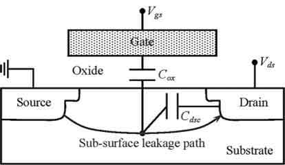
The structure of MOSFET is dependent on variations in the flow of carriers and the electrical variations in the channel width. Charge carriers enter the channel through the source terminal and exit through the drain. The voltage across the gate electrode, which is located between the source and drain, controls the width of the channel. The MOS is important because it can control the power flowing through it and its conduction current is limited. The following sections will discuss some of the most common applications for this type of device.

MOSFETs are used in a variety of applications. Some of these uses are as a high-frequency amplifier and in diagram showing how mosfets workvoltage regulator circuits. In some electronic circuits, they can also be used as a passive element. As a result, it can be used as a resistor or inductor. It is also commonly used as a DC relay and DC brushless motor drives. However, these applications are not the only ones.

MOSFETs are a type of semiconductor that works by controlling the flow of current and voltage between the source and drain terminals. Their main part is a MOS capacitor. It controls the flow of electrons and holes in a circuit. A MOSFET can be a p-type or n-type device. There are many different kinds of these semiconductors. Some are conductive, while others are non-conductive.

The MOSFET is used to switch between two different voltages. A single MOSFET can switch nearly 100 amps at low voltages. Some can handle up to 1000 V at lower currents. It is a versatile semiconductor that can be used in different electronic projects. It is available in many applications, including automotive, communications, computing, and consumer. It is a versatile semiconductor that is commonly found in electronic devices.

A MOSFET is a semiconductor that works as an electronic switch. It has four terminals and operates between the cut-off and saturation regions. It controls the current flow between the source and drain using a gate voltage. The gate electrode is located between the source and the drain. The gate electrode controls the width of the channel. A positive change in gate voltage produces an enhancement-mode. A negative change in the gate voltage produces an inverting effect.

It is used as a voltage regulator and high-frequency amplifier. Its high switching speed and low switching time make it an ideal device for low-power high-frequency converters. Its low power consumption, fast switching, and low heat generation make it a preferred semiconductor for many electronic projects. These include light intensity control, motor control, and max generators. By using MOSFET, circuit designers can save energy and lower the cost of their products.

In addition to controlling the current and voltage, MOSFETs are used in a variety of other applications. A MOSFET is used in various types of electrical appliances. Some examples of the devices that use MOSFETs are a DC motor, an electric motor, a switch, or a switch in a power outlet. The channel resistance is important for regulating the voltage and current flowing through the circuit.

The MOSFET is a semiconductor that converts electrical current to electricity in the same way that an inductor does. It is used in electrical and electronic projects that require high-frequency operation. Some of the most common devices that use MOSFETs include a power supply, an audio amplifier, a DC motor control, and a switch mode power supply. A MOSFET can also be used as a passive element, such as a resistor or inductor.

The MOSFET is a semiconductor that is used in electronics. Its main function is to control the current and voltage between the source and drain terminals. It is also used in many consumer products, including a power supply. A MOSFET has four terminals: the source (S), the drain (D), and the body (B). It works by varying the width of its channel. The device can be very small, or large.

A MOSFET has a MOS capacitor, which is its most important part. A MOSFET has two terminals, called the drain and the source. The source is connected to a conductive network, while the drain is a conductive channel. In order to change current, the negative gate voltage has a positive or negative effect. It has a negative impact on the electrical supply. A MOSFET is often used in the semiconductor industry.

Can you Deposit Metal Films on Sapphire Wafers?

Researcher Questions

We are wondering if your company can fabricate metal thin films on your sapphire wafers. We are looking for providers of thin films on sapphire of the general structure: sapphire (base) - metal M (5-20nm) - Au (500-1000 nm). here, a thin metal of element M (where M can be a range of different types of metal) of thickness 5-20nm, encapsulated by a thick layer of gold. the deposition needs to be done sequentially and immediately, so the metal M does not come into contact with ambient before being protected my the gold layer. we are looking for high purity metal depositions. another question we have is whether you have the capacity to deposit thin films of metallic borides or alternatively of elemental boron? this would also be of interest for us. 

Answer:

UniversityWafer, Inc. can deposit, by sputtering or Electron Beam Evaporation thin films of various metals (such as Ti, Fe, Cu, Ni, W, Cr) and then a film of Au.

In the EBEv equipment we can deposit on 4"Ø wafers layers of several different metals without having to open the reactor.
In the sputtering reactor we can do the same but we might be more limited as to our choice of targets.

The inner metal films should be at least 20nm thick to assure uniform covering of the substrate.

I think that depositing a film of Boron is not a problem although for sputtering we might not have such a target.

Metal Borides are not a fundamental problem provided they do not dissociate during EB evaporation, and not a problem for sputtering provided we have appropriate targets.

I do not know off-hand if there are any problems with the various metals adhering to Sapphire.

Minimum Order Quantity for each type of film structure is 8 of 4"Ø wafers for EVEv and either 1 or 22 4"Ø wafers for sputtering (depending on the reactor used).

We await your specifications

Wafers Quoted

  • Orientation: <0001> (C-plane)
  • Dimension: Dia. 2"x0.5 mm
  • Polishing: Single side polished
  • Roughness: Front-side Ra<0.5nm, Back-side Ra<1um
  •  5~20um (Ti or Cr) + 100nm Au on Back-side

Sapphire Wafers as Gallium Arsenide Grind/Polish

Research clients have used 100mm sapphire wafers 800 micron thick. The researchers used the wafer as a backing wafer for GaAs grinding/polish process. Rest of the spec same as you standard product: 2562. C-M plane 0.2°, Double Side Polished, Micro-roughness: Ra<0.35nm, Primary flat length: 32.5±2.5mm. Warp<21um, TTV<16um. The resercher purchased the following item.

Sapphire Item #2562
100mm <0001> 650um DSP C-M plane 0.2°, Double Side Polished, Micro-roughness: Ra<0.35nm, Primary flat length: 32.5±2.5mm. Warp<21um, TTV<16um

What Sapphire Wafer Spec Should I Use for Thin Film Research & Development?

Research scientists have used the following sapphire specifications for their thin film research.

Sapphire Item #1251
50.8mm 430um DSP C-M plane 0.2 Deg

What Sapphire Wafers can be used for Mid-Infrared Applications

We are using it for the mid-infrared applications. So is it possible to have 1~2 piece of sapphires (1cm*1cm) for us to test the optical properties? Just the same sapphire wafer as "C- plane, 1cm x1cm x430um thick, Double side polished, Ra<1nm " as we usually purchased before? We would like to make sure the infrared optical permittivity before we buy a lot more wafers. Let me know if it is possible to have 1~2 pieces of 1cm*1cm*430um samples.

C-plane<0001> sapphire substrate
Double side polish
Size 1cm*1cm / SQ 10X10mm
Thickness 300~500 um +/-25um
Surface roughnesss < 1nm Ra

Contact us for pricing.

Why is Sapphire Used in LEDs?

Sapphire is a chemically resistant material that is commonly used in LEDs. The main reason for using sapphire in LEDs is its ability to reflect light. As a result, manufacturers can produce patterned substrates. They begin with a blank sapphire and then etch it to produce a pattern. This process is commonly called plasma dry etching. The disadvantages of this technique include low etch rates and poor etched mask selectivity.

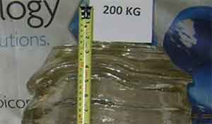
Since sapphire is transparent, LED makers can deposit gallium nitride onto the wafers. This processwhat does a sapphire wafer ingot look like helps LEDs generate light from multiple surfaces. This is unlike packaged LEDs, which only emit light from a single surface. The packaging of an LED allows the light to be collected from the top surface, which makes it difficult to see. Because sapphire is transparent, it is the best material to use as a substrate for LEDs.
The main advantages of sapphire are its cost and industry expertise. It is also inexpensive, which makes it the most cost-effective material for making LEDs. It also allows manufacturers to produce inexpensive LEDs. But sapphire has its drawbacks. Compared to silicon, it has a thermal mismatch, lattice mismatch, and poor electrical conductivity. For these reasons, it is best not to use sapphire in LEDs.

Another disadvantage is its incompatibility. As silicon has failed to replace sapphire as a substrate, the manufacturers use silicon instead. In addition, they tend to use cheaper materials such as glass or plastic, which is not compatible with LED production. A lot of LEDs are produced using silicon, so sapphire is the least expensive. These factors, however, are just as important as the advantages.

Sapphire is also better than other substrates for LEDs. The reason for this is because it has a higher optical transmission rate than silicon. As a result, LEDs can have a much higher light output. This is a major advantage of sapphire over silicon. The downside of silicon is its low cost. But this is also a drawback of sapphire. The material is not suited for LEDs due to the high price and high temperature of the production process.

LEDs are the most popular applications for sapphire. The material is transparent and is an excellent conductor of light. In comparison, silicon is opaque and does not allow for efficient light extraction. The semiconductor material is ideal for LEDs, however, because it is both cheap and transparent. This makes it a great choice for LEDs. But a sapphire substrate has a low cost, making it a popular choice for this technology.

According to IHS Technology, sapphire is the most popular substrate material. It is cheap and readily available. Its high-quality properties make it the ideal substrate material for LEDs. Its low cost is an advantage, but it comes with disadvantages. For example, it has high electrical resistance. So it is not the best substrate material for LEDs. But it has its advantages. The downside is that it is not as durable as silicon.

While silicon has been the dominant sapphire application, the use of sapphire is becoming more prevalent. Its advantages over other semiconductor materials include its cost and availability of silicon. The cost of sapphire has made it the best choice for LEDs, and it is a common material in LEDs. The main advantage of sapphire is that it is inexpensive. This is the most attractive feature of sapphire.

Besides being cheap, sapphire also has advantages in terms of transparency. The high transparency of sapphire makes it an excellent material for LEDs. Its low cost makes LEDs cheap to produce. It is a great material for light-emitting diodes. While it may be more expensive, it is an excellent material for LEDs. There are disadvantages to sapphire though, including its lattice mismatch, thermal incompatibility, and electrical conductivity.

For example, patterned sapphire substrates can improve light extraction efficiency. The polygonal pyramid shapes of these substrates help enhance light extraction. It is also more durable than plain sapphire. The commercial Prism LED is a better option. The faceted pattern is more expensive, but is better for the LED. It also requires less power. A good alternative is a crystalline-Sapphire LED.