SoN Wafers With Multiple Cavities
A professor of Electrical and Computer Engineering department requested a quote for the following.
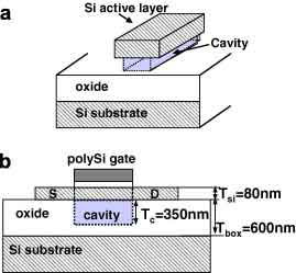
Silicon on nothing wafer which should have multiple cavities of few millimeters length buried inside Silicon.
Diameter is 100mm silicon wafer
P type Si wafer with 100 orientation
The wafer should have multiple SON structures separated from each other. Each of these SON should have a size of 2-3 mm^2.
I would like to know to order with these specifications what will be cost and how long will it take to deliver?
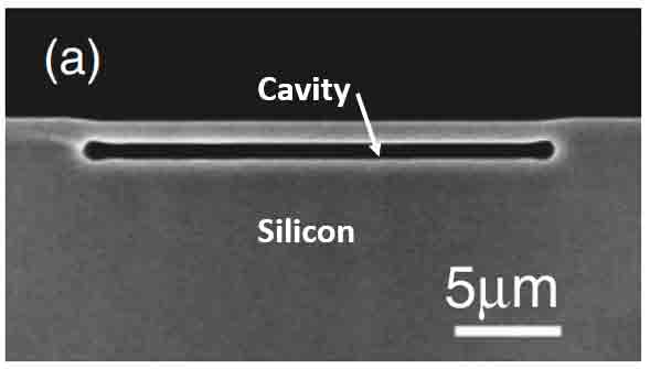
I have attached a SEM picture of typical SON structure. It is basically inbuilt cavity inside Si wafer.

Please let me know if it is possible to provide SON wafer. The quantity might depend on the costing of it.
Reference #301927 for specs and pricing.
Get Your SON Quote FAST! Or, Buy Online and Start Researching Today!
Where to Buy Silicon-on-Nothing (SON) Wafers
In the present invention, the formation of semiconductor devices with Silicon-on-Nothing (SON) technology is described. Such devices are fabricated on a semiconductor wafer using thin films of material, which are then patterned to form an integrated circuit. These SON devices have high on-current and low sub-threshold slope. This new technology can be easily applied to various fields, including biomedical and computer applications. This new process has several advantages over conventional etching processes.
What are Silicon-on-Nothing Advantages

As its name suggests, Silicon-on-Nothing (SON) structures are formed in the annealing process of a semiconductor. They are considered to be an efficient way to develop hollow materials. Previous studies have demonstrated the mechanism of SON structure formation. The surface energy minimization drives diffusion. During the annealing process, SON structures exhibit a wide variety of morphologies. Besides, SON structures are designed in cavities.
Unlike Silicon-on-Insulator (SOI) devices, SON devices have higher resolution and uniformity. Their unique architecture allows them to be fabricated using a thin silicon film and a buried dielectric. In a SON device, the buried dielectric, which may be an oxide or air gap, is fabricated on the front side of the silicon wafer. In addition, the device's performance is higher than that of SOI devices.
SON devices are a promising new approach to CMOS technology. They use ultra-thin silicon films to create sensors. In order to create these devices, an array of silicon trenches is annealed in a hydrogen environment to form a continuous crystalline layer over a vacuum cavity. This technique has been successfully applied in capacitive pressure sensors and other sensor applications. In this paper, a piezoresistive barometric pressure sensor is fabricated using the ESS process.
The fabrication of SON devices is based on a silicon-on-nothing substrate. The thinned BOX reduces source-to-drain coupling. The ground plane contact allows the semiconductor to fine-tune the threshold voltage. This method has numerous advantages, which have prompted its use in semiconductor technology. In addition, it offers high-quality and efficient devices. It is also scalable, which means it can be produced for various applications.
The first step is to create the thin box. However, this is easier said than done, and there is no room for mistakes. Because the process of silicon on nothing is faster, it can be used for multiple applications. So, it is a good candidate for RF integrated circuits. This technology offers a variety of advantages, including a high resistivity substrate. In addition, it is less expensive than traditional CMOS. So, it is scalable and can be scaled easily.
It is a low-cost alternative to bulk CMOS. It is a low-power solution to low-voltage applications. Unlike CMOS, silicon on nothing can operate at high frequencies. It is a low-power and flexible semiconductor, which means it can be manufactured in a wide range of sizes. The technology has the potential to provide a variety of applications, including radio frequency. With the right process, it will produce devices that work at high frequencies.
The second type of semiconductor structure has a high-frequency GIFBE. In this process, the top silicon layer is grown in layers that are between three and 100 nm thick. The bottom silicon layer is a layer that is less sensitive to heat than the upper silicon layer. In a similar way, this technology has the potential to revolutionize the way semiconductors are made. In fact, it may be the next step in advancing the field of nanotechnology.
SON combines the advantages of SOI and bulk devices. SON eliminates the disadvantages of SOI, including self-heating and poor Ion/Ioff trade-off. It has excellent S/D series resistance and a close-to-ideal subthreshold slope. It has several benefits over SOI, and may be used in ultimate device dimensions of 30 to 50 nm. It has been used to manufacture semiconductors.

