Research Requirements
- Quantum Hall measurements at 4 K
- Magnetic field up to 6 Tesla
- Carrier density around 1011 cm-2
- Carrier mobility near 105 cm²/V·s
- One research wafer for Hall bar fabrication
Discover how Hall effect sensors use silicon wafers and other semiconductor materials to measure magnetic fields, current, position, speed, and carrier transport. Learn which substrates are best for carrier mobility, carrier concentration, GaAs quantum Hall experiments, and semiconductor device fabrication. UniversityWafer supplies research-grade silicon, GaAs, germanium, and other advanced substrates for Hall effect measurements, Hall bar fabrication, magnetic sensor development, spintronics, and university research.

Researchers use silicon wafers, GaAs wafers, and other semiconductor substrates to fabricate Hall effect devices, characterize electrical properties, and study carrier transport. Selecting the proper substrate depends on the desired carrier concentration, carrier mobility, crystal orientation, resistivity, and operating temperature.
UniversityWafer supplies research-grade wafers for Hall effect measurements, Hall bar fabrication, quantum transport experiments, spintronics, and magnetic sensor development. Whether your project requires a single prototype wafer or production quantities, we can provide standard or custom specifications.
A university professor requested a GaAs/AlGaAs quantum well wafer for undergraduate laboratory experiments involving the Quantum Hall Effect. The goal was to fabricate Hall bars and perform electrical transport measurements at cryogenic temperatures.
Research Requirements
UniversityWafer Supplied
One 4-inch GaAs/AlGaAs quantum well wafer suitable for Quantum Hall Effect experiments and educational Hall bar fabrication.
Reference #323549
Get Your Hall Effect Wafer Quote FAST! Or, Buy Online and Start Researching Today!
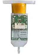
Hall effect sensors are widely used for position sensing, speed detection, current measurement, proximity sensing, and motor control. One familiar example is the BLTouch automatic bed-leveling sensor used in 3D printers, which relies on Hall effect technology to accurately detect probe movement.
Research-grade silicon wafers are commonly used to fabricate Hall effect devices because they offer excellent electrical properties, CMOS compatibility, and low manufacturing costs.
A researcher developing a custom Hall measurement system requested silicon wafers with known electrical properties to verify measurements of carrier concentration and carrier mobility.
UniversityWafer offered multiple characterization options including Hall measurements, resistivity testing, wafer thickness verification, and optional ECV analysis for accurate dopant profiling.
Reference #262959
UniversityWafer also supplies left- and right-handed α-quartz wafers for research involving spintronics, chiral phonons, and the inverse Hall effect. Available orientations include X-cut and Z-cut with optical-grade double-side polished finishes.
Reference #321539
For university laboratory courses, germanium wafers remain an excellent material for demonstrating Hall Effect principles because of their relatively high carrier mobility.
Typical Requested Specifications
Reference #277224
A Hall effect sensor is a semiconductor device that detects magnetic fields by measuring the voltage generated when an electric current passes through a material exposed to a magnetic field. This phenomenon, known as the Hall Effect, allows engineers to accurately measure magnetic field strength, current, position, speed, and proximity without physical contact.
Hall effect devices are commonly fabricated on silicon wafers, although specialized applications may use GaAs, InSb, or other compound semiconductors to improve sensitivity.
| Material | Advantages | Typical Applications |
|---|---|---|
| Silicon (Si) | Low cost, CMOS compatible | Automotive, industrial sensors |
| Gallium Arsenide (GaAs) | High electron mobility | Quantum Hall research |
| Indium Antimonide (InSb) | Very high sensitivity | Precision magnetic sensing |
| Indium Arsenide (InAs) | Excellent low-field performance | Scientific instrumentation |
Hall sensors are found in thousands of electronic products because they provide reliable, contactless magnetic field detection.
Although Hall effect sensors remain extremely popular, many next-generation systems now use Tunnel Magnetoresistance (TMR) sensors because they offer significantly higher sensitivity while consuming less power.
| Feature | Hall Effect | TMR |
|---|---|---|
| Sensitivity | Medium | Very High |
| Power Consumption | Higher | Very Low |
| Cost | Lower | Higher |
| Typical Uses | Automotive, industrial | MRAM, robotics, precision sensors |
Giant Magnetoresistance (GMR) sensors bridge the gap between Hall Effect and TMR technologies. They provide greater sensitivity than Hall sensors while remaining less expensive than many TMR devices.
| Technology | Sensitivity | Typical Applications |
|---|---|---|
| Hall Effect | mT range | Current sensing, automotive |
| GMR | μT range | Hard drives, industrial sensing |
| TMR | nT–μT range | MRAM, medical devices, robotics |
Despite advances in TMR and GMR technologies, silicon remains the most widely used substrate for Hall effect sensor fabrication because it offers excellent process compatibility with CMOS manufacturing, low production costs, and high reliability. Silicon Hall devices are used in millions of automotive systems, industrial controllers, smartphones, and consumer electronics every year.
UniversityWafer supplies research-grade silicon wafers, GaAs wafers, and other semiconductor substrates for Hall effect measurements, carrier mobility characterization, magnetic sensor development, spintronics, and quantum transport research.