
Silicon Wafers for SU-8 Lithography
Silicon wafers are widely used as substrates for SU-8 lithography, MEMS, microfluidics, sensors, electroplating molds, and other microfabrication processes. Their flat, polished surfaces provide a stable platform for spin coating, UV exposure, development, and fabrication of thick, high-aspect-ratio SU-8 structures.
SU-8 is an epoxy-based negative photoresist. During exposure, a photoacid generator produces acid in illuminated regions. During the post-exposure bake (PEB), the acid catalyzes cationic crosslinking of the epoxy groups. The crosslinked exposed regions become substantially less soluble in the developer, while properly processed unexposed material is removed during development.
Substrate selection can influence coating uniformity, adhesion, exposure behavior, thermal stress, feature quality, and compatibility with downstream fabrication. Researchers should therefore select the wafer together with the SU-8 formulation, target resist thickness, feature dimensions, exposure system, and subsequent process steps.
Choosing a Silicon Wafer for SU-8 Lithography
There is no single silicon wafer specification required for every SU-8 process. Important parameters can include wafer diameter, thickness, orientation, surface finish, flatness, resistivity, conductivity type, and any dielectric or thin-film layers present on the surface.
- Wafer Diameter: Common laboratory sizes include 2 inch, 3 inch, 100 mm (4 inch), and 150 mm (6 inch). The diameter should match the spin coater, mask aligner, hotplate, chuck, and other fabrication equipment.
- Surface Finish: A polished device surface is generally preferred because low roughness and good flatness support uniform photoresist coating and lithographic patterning.
- Wafer Thickness: Thickness should be compatible with wafer handling, vacuum chucks, mask aligners, spin coaters, and downstream processing equipment.
- Crystal Orientation: Si(100) is common in MEMS and microfabrication. Orientation may become especially important when crystallographically anisotropic silicon etchants are used after lithography.
- Resistivity and Conductivity Type: These specifications may be relatively unimportant when the wafer serves only as a mechanical mold substrate, but they can be critical when the silicon forms an electrical part of a sensor, MEMS, or microelectronic device.
- Surface Layers: Bare silicon, thermal SiO2, silicon nitride, metals, and other thin films can alter adhesion, optical reflectivity, electrical isolation, and downstream etch behavior.
Single-Side vs. Double-Side Polished Silicon
Single-side-polished (SSP) silicon wafers are suitable for many conventional SU-8 processes in which only the front surface is coated and patterned.
Double-side-polished (DSP) silicon wafers can be useful when the process involves backside alignment, through-wafer optical access, wafer bonding, backside lithography, or processing on both wafer surfaces.
SU-8 Surface Preparation and Adhesion
Surface cleanliness and dehydration are important for reliable SU-8 coating and adhesion. Particles can create coating defects, while organic contamination or adsorbed moisture can contribute to poor adhesion and pattern defects.
Before coating, substrates are commonly cleaned and dehydrated according to the requirements of the substrate and selected SU-8 formulation. Processing conditions should follow the current photoresist manufacturer's recommendations because bake temperature, bake time, exposure dose, development conditions, and resist thickness are interdependent.
Adhesion also depends on the underlying surface. Bare silicon, SiO2, silicon nitride, glass, and metal films do not necessarily interact with SU-8 in the same way. Surface treatments or adhesion promoters may be useful for some material systems, but they should be qualified for the specific fabrication process rather than assumed to be universally necessary.
SU-8 Coating and Film Thickness
One of SU-8's major advantages is its ability to produce relatively thick patterned photoresist layers. Available SU-8-family formulations span a wide viscosity range, allowing film thickness to be adjusted through resist formulation and coating conditions.
Spin-coated thickness depends on factors such as resist viscosity, spin speed, acceleration, coating time, substrate geometry, and processing conditions. Very thick films may require carefully controlled soft-bake and post-exposure-bake schedules to reduce solvent gradients and excessive internal stress.
The exact achievable thickness and recommended processing window should always be determined from the technical data for the specific SU-8 formulation being used.
Why SU-8 Is Used for High-Aspect-Ratio Structures
SU-8 is well known for fabricating thick microstructures with comparatively high aspect ratios and near-vertical sidewalls when exposure, focus, bake, and development conditions are properly optimized.
Its epoxy chemistry produces mechanically robust crosslinked structures, making patterned SU-8 useful not only as a photoresist but also as a permanent structural material or master mold in selected applications.
Maximum practical aspect ratio depends on the feature geometry, resist thickness, exposure optics, mask quality, substrate reflectivity, adhesion, development, and process optimization. It should therefore not be treated as a single universal value for all SU-8 processes.
Thermal Oxide Wafers for SU-8 Lithography
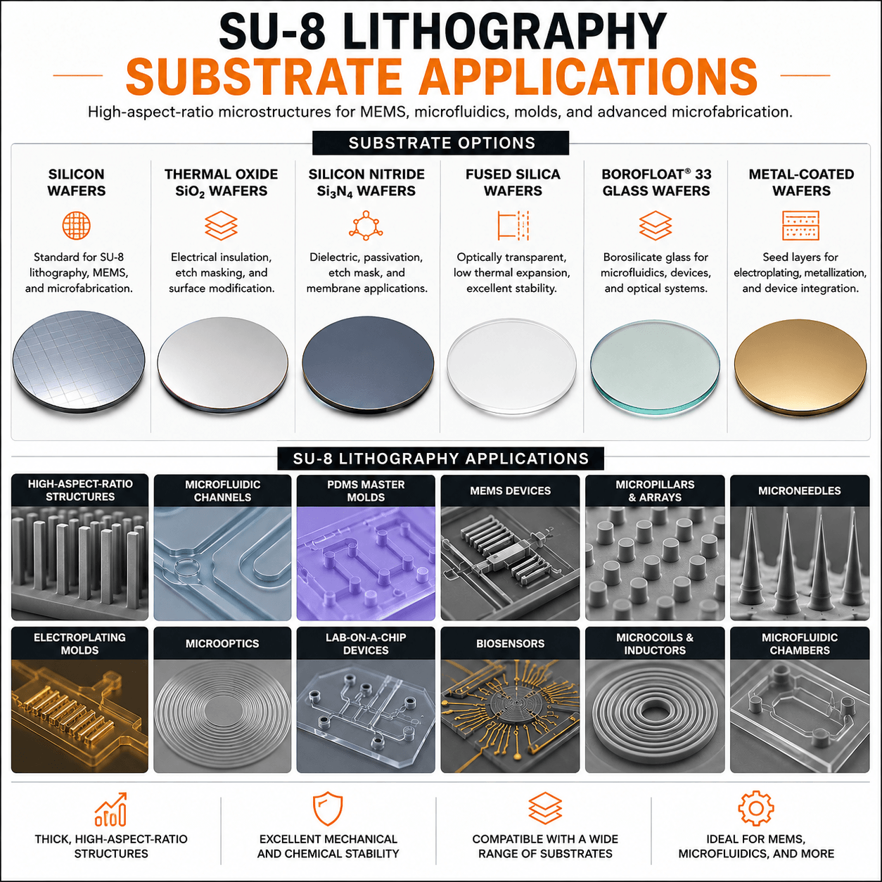
Thermal oxide silicon wafers contain a silicon dioxide (SiO2) layer grown on the silicon substrate. Oxide-coated wafers are useful when a fabrication process requires electrical isolation, a dielectric layer, an etch mask, or particular optical or surface properties.
Thermal oxide thickness should be selected for its function in the device rather than simply for the SU-8 coating itself. Researchers should consider whether the SiO2 will remain in the final structure or serve as a temporary masking, isolation, sacrificial, or processing layer.
Silicon Nitride Wafers for SU-8 Microfabrication
Silicon nitride on silicon is another useful substrate system for MEMS and microsystem fabrication. Depending on its deposition method and properties, SiNx can function as a dielectric, passivation layer, etch mask, membrane, or structural thin film.
When SU-8 patterning is combined with wet etching, dry etching, thin-film deposition, or membrane fabrication, the nitride composition, thickness, residual stress, and etch selectivity should be considered as part of the complete process flow.
Glass and Fused Silica for SU-8 Lithography
SU-8 can also be patterned on transparent substrates when optical access through the substrate is useful. Glass-based substrates are common in microfluidics, optical microsystems, sensors, and lab-on-chip research.
Fused silica wafers provide high optical transparency over a broad spectral range, low thermal expansion, and good dimensional stability. These properties can be useful for optical, photonic, and microfluidic applications.
Borofloat glass is another substrate option for microfluidic and microsystem fabrication when borosilicate glass properties are appropriate for the process.
When exposing SU-8 on transparent substrates, the optical properties of the substrate and any underlying films can influence exposure through reflection, transmission, and standing-wave effects. These effects become increasingly important when tight dimensional control is required.
SU-8 for Microfluidic and PDMS Master Molds
One of the most common applications of SU-8 is fabrication of master molds for microfluidic devices . Photolithographically patterned SU-8 can define channels, chambers, pillars, wells, and other microscale features.
The patterned SU-8 master can then be used in soft lithography to replicate its topography into an elastomer such as polydimethylsiloxane (PDMS). After curing, the replicated PDMS structure is separated from the master and can be incorporated into a microfluidic device.
Polished silicon is particularly useful as a master substrate because it provides a flat, mechanically stable surface and is compatible with established cleanroom photolithography equipment.
SU-8 Lithography for MEMS
In microelectromechanical systems (MEMS), SU-8 can serve as a patterned structural polymer, mold, spacer, masking material, or component of a larger fabrication sequence.
Applications can include microsensors, microfluidic components, micromechanical structures, micro-optical elements, electroplating molds, and experimental MEMS devices.
Silicon remains a particularly useful MEMS substrate because it is compatible with established microfabrication techniques including UV lithography , thin-film deposition, oxidation, dry etching , and wet chemical etching.
Mechanical Grade Silicon for SU-8 Process Development
Not every SU-8 experiment requires prime semiconductor-grade silicon. Mechanical grade silicon wafers may provide a lower-cost option for selected coating trials, spin-process development, equipment testing, handling experiments, training, or educational applications.
Mechanical-grade wafers should not automatically be substituted for prime wafers when surface defect density, contamination, flatness, electrical properties, or tight lithographic control are important. Surface finish, thickness, bow, warp, diameter, and equipment compatibility should still be verified before use.
Common SU-8 Lithography Applications
- High-aspect-ratio microstructures
- MEMS fabrication
- Microfluidic master molds
- PDMS soft-lithography molds
- Lab-on-a-chip research
- Microchannels, chambers and micropillars
- Microsensors and microactuators
- Electroplating molds
- Microneedle research
- Micro-optical structures
- Microfabrication process development
Silicon Wafers for SU-8 Research
UniversityWafer supplies silicon, oxide-coated, nitride-coated, glass, and specialty wafer substrates for SU-8 lithography, MEMS, microfluidics, photolithography, and microfabrication research.
When requesting a substrate, specify the required wafer material, diameter, thickness, orientation, resistivity, conductivity type, surface finish, coating or dielectric layer, and quantity. If the substrate will undergo backside alignment, etching, wafer bonding, or other downstream processes, those requirements should also be included.
Get Your SU-8 Lithography Wafer Quote FAST!
Or,
Buy Wafers Online
and start researching today!
How Does SU-8 Lithography Work?
SU-8 lithography is a negative-tone photolithography process used to fabricate thick and high-aspect-ratio polymer microstructures. SU-8 is based on multifunctional epoxy chemistry and contains a photoacid generator that responds to ultraviolet exposure.
During UV exposure through a photomask, photoacid is generated primarily in the illuminated regions. A subsequent post-exposure bake (PEB) promotes acid-catalyzed cationic ring-opening polymerization and crosslinking of the epoxy groups.
After development, properly crosslinked exposed regions remain on the substrate while the unexposed resist is removed. This negative-tone behavior enables SU-8 to form mechanically robust microstructures with relatively high aspect ratios.
SU-8 is widely patterned on silicon wafers , glass, fused silica, oxide-coated silicon, and other substrates for microfabrication research.
Typical SU-8 Lithography Process
A typical SU-8 process includes several carefully controlled steps. Exact temperatures, times, spin speeds, exposure doses, and development conditions depend on the specific SU-8 formulation, film thickness, substrate, exposure equipment, and desired feature geometry.
- Substrate Preparation: Clean and dehydrate the wafer to reduce contamination and surface moisture that can interfere with coating or adhesion.
- SU-8 Coating: Apply the photoresist, commonly by spin coating. Resist viscosity and coating parameters are selected according to the target film thickness.
- Soft Bake: Heat the coated substrate to remove a controlled amount of solvent and stabilize the film before exposure.
- UV Exposure: Expose the SU-8 through a photomask. The exposed regions generate the photoacid needed for subsequent crosslinking.
- Post-Exposure Bake: Heat the exposed resist to promote acid-catalyzed epoxy crosslinking in the exposed regions.
- Development: Remove unexposed SU-8 using a developer appropriate for the selected resist system.
- Rinse and Dry: Rinse according to the process specification and dry the patterned wafer while minimizing damage to delicate structures.
- Optional Hard Bake: Some applications use an additional thermal treatment when increased mechanical or chemical stability is desired. This step is application-dependent and is not required for every SU-8 process.
Process parameters should be taken from the current technical documentation for the particular SU-8 formulation rather than using one universal recipe.
SU-8 UV Exposure and Crosslinking
SU-8 formulations are commonly processed using near-UV lithography. Exposure activates the photoacid generator, but the principal crosslinking reaction is promoted during the post-exposure bake.
Exposure dose must be sufficient to generate the photoacid needed through the desired resist thickness. Underexposure can produce incomplete crosslinking, weak features, or poor pattern retention, while excessive exposure can contribute to dimensional changes or loss of feature fidelity.
The optimum dose depends on resist formulation, thickness, exposure wavelength, optical system, substrate reflectivity, mask contact, and feature geometry.
Why Is the Soft Bake Important?
After coating, SU-8 contains solvent that must be reduced before exposure. The soft bake helps stabilize the resist film and establish appropriate solvent content for subsequent lithography.
Bake conditions become particularly important for thick SU-8 films. Excessively rapid heating or cooling, inappropriate bake times, or strong solvent gradients can contribute to internal stress, nonuniform processing, adhesion problems, or cracking.
Thick films may therefore benefit from controlled thermal ramps and careful temperature management according to the resist manufacturer's recommended process.
Why Is the Post-Exposure Bake Important?
The post-exposure bake (PEB) is a critical chemical step in SU-8 lithography. Photoacid generated during UV exposure catalyzes crosslinking of the epoxy groups as the film is heated.
Proper PEB conditions help establish sufficient crosslink density in the exposed regions so that they survive development. Temperature history can also influence stress and dimensional fidelity, especially in thick or high-aspect-ratio structures.
SU-8 should therefore not be described as requiring days or months to complete the lithographic crosslinking process. In conventional processing, exposure and PEB are deliberately engineered to produce the required crosslinked image within the fabrication sequence.
Developing SU-8 Photoresist
Development removes the unexposed, sufficiently uncrosslinked resist while leaving the exposed and crosslinked pattern on the substrate.
SU-8 processes commonly use solvent-based developers such as propylene glycol monomethyl ether acetate (PGMEA), depending on the formulation and manufacturer's recommendations.
Development time depends strongly on film thickness, feature geometry, agitation, developer condition, and degree of crosslinking. Incomplete development can leave residual resist in channels and openings, while excessive or mechanically aggressive processing can damage delicate structures.
SU-8 Film Thickness and Aspect Ratio
A major advantage of SU-8 is its ability to form thick photoresist films and high-aspect-ratio structures. This makes it useful for structures that can be difficult to fabricate with conventional thin photoresists.
Aspect ratio is commonly expressed as the relationship between feature height and lateral dimension:
Aspect Ratio = Feature Height / Feature Width
Practical aspect ratio is not determined by SU-8 chemistry alone. It depends on resist thickness, mask design, exposure optics, diffraction, substrate reflection, adhesion, development, feature spacing, and mechanical stability.
Consequently, very high aspect ratios reported for optimized research processes should not be treated as guaranteed values for every SU-8 structure.
Common SU-8 Lithography Problems
SU-8 can produce excellent structures, but thick-resist processing requires careful control. Common issues include:
- Poor Adhesion: Can result from contamination, moisture, incompatible surface chemistry, or excessive stress.
- Cracking: Can be associated with residual stress, thick films, thermal history, substrate mismatch, or aggressive bake conditions.
- Edge Bead: Thick resist can accumulate near the wafer edge during spin coating, affecting mask contact and exposure uniformity.
- Incomplete Development: Residual unexposed resist can remain when development conditions are insufficient for the film thickness and geometry.
- Feature Collapse: Tall, narrow structures can deform or collapse because of mechanical instability and capillary forces during liquid drying.
- Sidewall or Dimensional Errors: Exposure dose, diffraction, reflections, mask contact, and resist thickness can alter the final feature dimensions.
- Delamination: Interfacial stress or poor surface preparation can cause the patterned resist to separate from the substrate.
Preventing SU-8 Feature Collapse
Very tall or narrow SU-8 features can be mechanically vulnerable during development, rinsing, and drying. Collapse should not simply be attributed to the developer having a "high vapor pressure."
Capillary forces during liquid evaporation can pull closely spaced or mechanically compliant structures together. Feature geometry, crosslinking, adhesion, material stiffness, rinse procedure, and drying method all influence this behavior.
Researchers working near the mechanical limits of the structure may need to optimize spacing, exposure, PEB, development, and drying conditions.
Substrate Reflectivity and SU-8 Patterning
The material beneath the SU-8 layer can influence lithographic performance. Silicon, oxide, glass, metals, and other films have different optical properties at the exposure wavelength.
Reflections from the substrate can modify the optical intensity distribution within the resist and contribute to standing-wave or dimensional effects. These interactions can become especially important when fabricating thick resist layers or tightly controlled microstructures.
Substrate selection should therefore consider not only mechanical and electrical properties but also the optical behavior of the complete resist/substrate stack.
SU-8 Master Molds for PDMS Soft Lithography
SU-8 patterned on polished silicon is widely used to fabricate master molds for PDMS soft lithography. UniversityWafer's related microfluidic examples use patterned silicon masters to define channels and other structures that are subsequently replicated into PDMS. :contentReference[oaicite:1]{index=1}
A typical workflow is:
- Pattern SU-8 on a polished silicon wafer.
- Complete development to form the master topography.
- Cast liquid PDMS over the SU-8 master.
- Cure the PDMS.
- Separate the replicated PDMS layer from the master.
- Bond or assemble the PDMS structure into the final microfluidic device.
The SU-8 master can define microchannels, chambers, wells, pillars, and other structures used in lab-on-chip, organ-on-chip, biosensor, cell-culture, and microfluidic research. :contentReference[oaicite:2]{index=2}
SU-8 in MEMS Fabrication
SU-8 is also used in microelectromechanical systems (MEMS) as a structural polymer, spacer, mold, mask, or component of a multilayer device.
Its ability to form comparatively thick structures makes it useful for microchannels, mechanical structures, electroplating molds, optical components, and experimental sensors.
The final process must account for the chemical and thermal compatibility of crosslinked SU-8 with subsequent deposition, etching, bonding, cleaning, or packaging steps.
SU-8 for Electroplating Molds
Thick patterned SU-8 can function as a mold for electroplated metal microstructures. Openings in the patterned resist define regions where metal is deposited onto an underlying conductive seed layer.
This approach can be used to fabricate thick metal features for MEMS, microsystems, microcoils, and other microfabricated components.
For electroplating applications, researchers should consider SU-8 thickness, sidewall profile, seed-layer compatibility, adhesion, plating chemistry, and whether the resist must subsequently be removed.
Can SU-8 Be Used as a Permanent Material?
Yes. Although SU-8 is widely known as a photoresist, highly crosslinked SU-8 can also remain as a permanent polymeric component in selected microsystems.
Permanent SU-8 structures can function as spacers, microchannels, insulating structures, microfluidic components, mechanical features, and packaging elements.
Whether SU-8 should remain in the final device depends on the required thermal stability, chemical resistance, mechanical properties, electrical behavior, optical properties, outgassing requirements, and long-term reliability.
SU-8 vs. Positive Photoresist
SU-8 is a negative photoresist: exposed regions become crosslinked and remain after development. In a conventional positive photoresist process, exposure instead increases the solubility of the exposed regions in the developer.
| Property | SU-8 Negative Resist | Typical Positive Resist |
|---|---|---|
| Exposed Region | Remains after development | Removed during development |
| Film Thickness | Well suited to thick resist processing | Often used for thinner conventional lithography |
| High-Aspect-Ratio Structures | Major application | Depends strongly on resist system |
| Common Uses | MEMS, microfluidics, molds, structural features | Pattern transfer, etching, implantation, lift-off* |
*Lift-off performance depends strongly on the specific resist system and profile; this comparison is not intended to describe every positive photoresist.
SU-8 Lithography Applications
SU-8 lithography supports a broad range of microfabrication applications, including:
- High-aspect-ratio microstructures
- MEMS sensors and structures
- Microfluidic channels and chambers
- PDMS master molds
- Lab-on-a-chip devices
- Organ-on-chip research
- Biosensors
- Microneedle structures
- Electroplating molds
- Micro-optical structures
- Microcoils and microsystem components
- Permanent polymer microstructures
SU-8 Wafers for Microfabrication Research
UniversityWafer supplies silicon wafers , thermal oxide wafers, silicon nitride substrates, fused silica, Borofloat, and other substrates for SU-8 lithography, MEMS, microfluidics, and photolithography research.
Researchers should specify the required substrate material, diameter, thickness, surface finish, orientation, resistivity, dielectric layers, and downstream fabrication requirements when requesting wafers.
Related SU-8 Lithography & Microfabrication Resources
- SU-8 Photoresist – Learn about SU-8 negative photoresist, wafer selection, patterning and microfabrication applications.
- SU-8 Photolithography – Explore SU-8 processing on silicon and glass wafers for MEMS and microfluidic fabrication.
- SU-8 Molds for PDMS – Silicon wafer master molds for PDMS soft lithography and microfluidic device fabrication.
- PDMS Microfluidic Devices – Learn how SU-8 patterned silicon masters are used to fabricate PDMS microchannels and lab-on-chip devices.
- Silicon Wafers for Soft Lithography – Substrates for PDMS molds, microfluidics and replication-based microfabrication.
- Microfluidic Substrates – Silicon, glass and specialty substrates for microchannels, lab-on-chip systems and microfluidic research.
- Silicon Wafers – Polished silicon substrates for SU-8 lithography, MEMS, microfluidics and semiconductor research.
- Single-Side-Polished Silicon Wafers – Polished substrates suitable for many front-side SU-8 coating and lithography processes.
- Double-Side-Polished Silicon Wafers – DSP substrates for backside alignment, optical access and double-sided microfabrication.
- Thermal Oxide Silicon Wafers – SiO2-coated silicon substrates for dielectric, masking and microfabrication applications.
- Silicon Nitride Wafers – Nitride-coated substrates for MEMS, membranes, masking and microsystem fabrication.
- Fused Silica Wafers – Transparent substrates for optical, photonic and microfluidic SU-8 structures.
- Borofloat 33 Glass Wafers – Borosilicate glass substrates for microfluidics, MEMS and optical microsystems.
- UV Lithography – Learn how ultraviolet exposure transfers patterns into photoresist during microfabrication.
- Microfabrication – Explore lithography, deposition, etching and other processes used to manufacture microscale devices.