I would like to buy some (110) oriented Si wafers. I am thinking 1 mm thickness and 50 mm diameter. Can you please give me a quote for 10? I plan to use EDT to etch channels with vertical sidewalls into them. I am mentioning this because I am not sure if/how the other properties (dopant, resistivity, etc) will affect this process.
Substrates Used For Isotropic Etching
What Silicon Wafer Spec is Used for Isotropic Etching
A PhD candidate requested a quote for the following:
UniversityWafer, Inc. Quoted:
Si Item #4N1 25 wafer
2" N/Ph [110] 1,000um DSP FZ 15-18 ohm-cm 1 F @ <1,-1,0>
Reference #224327 for specs and pricing.
Get Your Silicon Wafer Quote FAST! Or, Buy Online and Start Researching Today!
Wet Isotropic Etching On Silicon Wafers
A postdoc requested a quote for the following:
We hope to buy some silicon wafers with pre-grown SiO2 on top, so could you please tell me whether your company provide such oxide growing service?
I also hope to know whether doping will influence the crystalline forms of SiO2 and wet isotropic etching on Silicon?
Yes, we can grow and have in stock silicon wafers with thermal oxide deposited onto them.
Reference #251174 for specs and pricing.
What Is Isotropic etching?
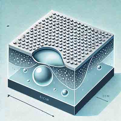
Isotropic etching is a process used in microfabrication and semiconductor manufacturing to remove material from a substrate in a manner that is uniform in all directions. This means that the material is etched away at the same rate vertically and laterally, resulting in rounded or undercut features.
Key characteristics of isotropic etching include:
- Uniform Removal: Material is removed uniformly in all directions, leading to the creation of rounded or non-vertical sidewalls.
- Chemical Etching: It is often achieved through chemical etching, where the etchant solution reacts with the material to dissolve it uniformly.
- Applications: Commonly used for creating features where precise control of sidewall angles is not critical or when rounded features are desired.
Isotropic etching is different from anisotropic etching, where material removal is directional, usually resulting in straight, vertical sidewalls.
What Substrate And Substrate Specs Are Often Used For Isotropic Etching?
In the context of isotropic etching, various substrates are used depending on the application, but here are some common substrates and their specifications:
Common Substrates:
-
Silicon (Si):
- Usage: Widely used in semiconductor manufacturing and MEMS (Micro-
 Electro-Mechanical Systems).
 - Specifications: Typically comes in wafer form with diameters ranging from 100mm (4 inches) to 300mm (12 inches). Thickness can vary from 200µm to 750µm or more, depending on the wafer diameter and application.
- Usage: Widely used in semiconductor manufacturing and MEMS (Micro-
-
Silicon Dioxide (SiO2):
- Usage: Often used as a sacrificial layer or mask in etching processes.
- Specifications: Can be thermally grown or deposited. Thickness can range from a few nanometers to several micrometers.
-
Silicon Nitride (Si3N4):
- Usage: Commonly used as an etch mask due to its resistance to many etchants.
- Specifications: Typically deposited via CVD (Chemical Vapor Deposition) with thicknesses ranging from tens of nanometers to a few micrometers.
-
Gallium Arsenide (GaAs):
- Usage: Used in optoelectronics and high-frequency applications.
- Specifications: Wafers typically range from 50mm to 150mm in diameter with thicknesses from 200µm to 600µm.
-
Quartz (SiO2):
- Usage: Used in optics and MEMS applications.
- Specifications: Comes in various forms, including wafers, with thicknesses typically ranging from a few hundred micrometers to several millimeters.
Substrate Specifications:
- Diameter: Depending on the material and application, substrates can range from small pieces to large wafers (up to 300mm for silicon).
- Thickness: Varies widely based on the application, from a few micrometers to several millimeters.
- Doping Type and Concentration: For silicon, substrates can be p-type or n-type, with various levels of doping to control electrical properties.
- Crystal Orientation: For silicon, common orientations include <100>, <110>, and <111>, which affect etching rates and surface properties.
- Surface Finish: Can be polished (single or double-sided) or unpolished, affecting the etching uniformity and subsequent processing steps.
These specifications are tailored to the needs of the specific etching process and the desired outcome of the fabrication steps.
