N-Type Silicon Wafers for Nanotube Fabrication
A graduate student requested a quote for the following substrates.
- Could you send me a quotation for silicon wafers (2” – 25 pieces), dopant N/P, Ori (100) or (111), resistivity 1-20 Ohm-cm,
- Silicon wafers (2” – 25 pieces), dopant N/P, Ori (100) or (111), resistivity 1-20 Ohm-cm,covered with a SiO2 layer of about 300-500 nm.
These wafers will be used as substrate for carbon nanotubes growth by CVD method.
Reference #160627 for specs and pricing.
Get Your Quote FAST! Or, Buy Online and Start Researching Today!
Carbon Nanotube Synthesis
A university postdoc requested a quote for the following.
Question:
We need the wafer as the substrate for Carbon Nanotube Synthesis. So the Ori, resistivity and dopant are not important measures for us. Is it possible to have the wafer in square? I would like to hear from you soon.
Answer:
Carbon nanotube (CNT) synthesis involves creating CNTs through methods like Chemical Vapor Deposition (CVD), Arc Discharge, and Laser Ablation. In CVD, carbon-containing gases decompose on metal catalysts at high temperatures, forming nanotubes. Arc Discharge uses an electric arc between carbon electrodes to vaporize carbon, which then condenses into nanotubes. Laser Ablation vaporizes a carbon target using a laser, with carbon atoms forming nanotubes as they cool. Each method aims to produce CNTs with specific properties, such as length, diameter, and purity, for applications in electronics, materials science, and nanotechnology.
Reference #99521 for specs and pricing.
Related Substrate Pages
What are Carbon Nanotubes?
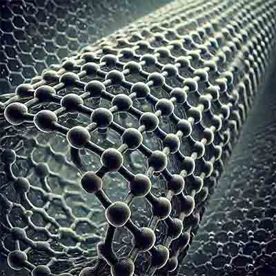
Nanotubes, specifically carbon nanotubes (CNTs), are cylindrical molecules made up of carbon atoms arranged in a hexagonal lattice, similar to the structure of graphite. These tubes have extraordinary properties due to their unique structure, including:
-
Strength: Carbon nanotubes are incredibly strong and have a very high tensile  strength, making them one of the strongest materials known.
-
Electrical Conductivity: They can be excellent conductors of electricity or semiconductors, depending on how the carbon atoms are arranged.
-
Thermal Conductivity: Nanotubes also have exceptional thermal conductivity, meaning they can transfer heat very effectively.
-
Flexibility and Elasticity: Despite their strength, carbon nanotubes are also flexible and can be bent without breaking.
-
Lightweight: Nanotubes are extremely lightweight, which makes them valuable for applications requiring high strength-to-weight ratios.
There are two main types of carbon nanotubes:
Single-Walled Nanotubes (SWNTs): Consist of a single layer of carbon atoms wrapped into a cylindrical shape.
Multi-Walled Nanotubes (MWNTs): Consist of multiple layers of carbon atoms wrapped into concentric cylinders.
These nanotubes have a wide range of potential applications, including in materials science, electronics, energy storage, and medicine, due to their unique properties.
What Substrates are Commonly Used to Fabricate Nanotubes?
Fabricating nanotubes, particularly carbon nanotubes (CNTs), often involves using substrates that provide a suitable surface for growth and adherence. The choice of substrate can influence the quality, alignment, and yield of the nanotubes. Some common substrates used for fabricating nanotubes include:
1. Silicon (Si)
- Silicon Wafers: Silicon wafers are widely used due to their availability, ease of processing, and compatibility with microelectronics. They often have a thin layer of silicon dioxide (SiO2) on the surface to enhance nanotube growth.
Carbon Nanotubes for Researching Organic Solar Cell Electrodes
A materials professor researching nanotubes requested a quote for the following.
Our research of the electrodes for organic solar cells, we need silicon wafers with elevated conductivity as the substrate for the grow of carbon nanotubes from deposited nano-nuclei of gold on the surface of the wafers. The wafers should have dimensions about 15x15 to 25x25 mm. Please, can you send me the proforma account for 50 - 100 wafers?
UniversityWafer, Inc. Quoted
Item Qty. Description
Q98b. 3/6 Silicon wafers, per SEMI, P/E 4"Ø×525±25µm,
p-type Si:B[100], Ro=(0.010-0.020)Ohmcm,
One-side-polished, back-side Alkaline etched, SEMI Flats (two),
Each wafer diced into at least 20 of 16×16mm squares, sides parallel to [110],
Shipped on dicing tape, in single wafer cassettes.
Reference #93970 for specs and pricing.
2. Silicon Dioxide (SiO2)
- Thermally Grown SiO2: Often used as a thin insulating layer on silicon wafers. The SiO2 layer can help control the growth of carbon nanotubes and serve as a barrier to prevent unwanted interactions with the underlying silicon.
Thermal Oxide Coated Silicon Wafers for Carbon Nanotube Growth
A faculty fellow requested a quote for the following.
We use the wafer for carbon nanotube growth, and actually we are not sensitive - most of the time - for the size, quality and doping of the silicon itself, but we would need wafers capped with thick oxide. If you have something on hand with oxide thickness between 500 nm and 2 micron, we would be interested. Please let me know if you have some good deal for this.
Also, we might need a smaller amount of similar materials but with double side polished surface.
Reference RFQ#84405 for specs and pricing.
3. Quartz (Silicon Dioxide, SiO2)
- Fused Quartz: Quartz substrates are used due to their high temperature stability and transparency, which can be beneficial in certain characterization techniques.
Electronic Grade Quartz Wafers for Growing Carbon Nanotubes
A Quantum Photonics researcher requested a quote for the following.
Question:
Do fused quartz substrates have the highest processing temperature? I would like to grow carbon nanotubes on them, growth temperature is 800C, do you think the substrate will stand this temperatures?
Answer:
Yes, fused quartz substrates are well-suited for high-temperature processes, including the growth of carbon nanotubes. Fused quartz has a very high melting point, around 1,670°C, and excellent thermal stability, which means it can easily withstand the 800°C growth temperature you are considering for carbon nanotube synthesis. This makes it an appropriate choice for your application.
Reference #114959 for specs and pricing.
4. Sapphire (Al2O3)
- Single-Crystal Sapphire: Sapphire is a popular choice because of its high melting point, mechanical strength, and ability to withstand the high temperatures used in nanotube synthesis.
5. Metal Substrates
- Nickel (Ni), Copper (Cu), and Cobalt (Co): These metals are often used as catalysts and substrates simultaneously.
6. Alumina (Al2O3)
- Alumina Substrates: These are sometimes used for their high thermal stability and resistance to chemical attack.
7. Glass
- Borosilicate Glass: Sometimes used for its transparency and heat resistance, glass substrates are more common in research settings rather than large-scale production.
The Best Glass Wafers to Grow Nanotubes On
A posdoc asked the following question.
Question:
I am looking for a substrate made of glass and I would like to know what is the difference between ITO Glass and Soda Lime Glass. I want to use this substrate to deposit carbon nanotubes and tested as field emitters.
Answer:
ITO glass and soda lime glass differ primarily in their composition and functionality. ITO glass (Indium Tin Oxide glass) is a conductive glass coated with a thin layer of indium tin oxide, making it transparent and electrically conductive. It is widely used in touchscreens, displays, and solar cells. Soda lime glass, on the other hand, is a common, non-conductive glass composed mainly of sodium oxide, lime, and silica.
Reference #234942 for specs and pricing.
8. Graphite and Graphene
- Highly Ordered Pyrolytic Graphite (HOPG)
- Graphene Substrates
9. Polymers
- Polymer Substrates: Certain polymers, such as polystyrene or polymethyl methacrylate (PMMA), can be used in fabricating nanotubes for specific applications.
The choice of substrate is crucial in determining the growth mechanism, alignment, and properties of the nanotubes, which in turn affects their suitability for various applications, ranging from electronics to composite materials.

 strength, making them one of the strongest materials known.