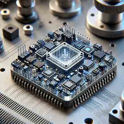
Thin Germanium Wafer, 3" dia, CA 2.5", 200±3um thick, flatness/ bow < 2um, thickness, uniformity<0.2um
Purpose: optical switch for regenerative CO2 laser amplifier
LightMachinery Inc. Item# OP-7035 Thin Germanium Wafer or its Equivalent:
QTY: 2
Substrates for Optical Micro-Electro-Mechanical Systems (MEMS)
Germanium Wafer Optical Switch For Regenerative CO2 Laser Amplifier
A postdoc requested a qutoe for the following:
Reference # for specs and pricing.
Get your Substrate Quote Today! Or, Buy Online and Start Researching Today!!
What Substrate Is Used to Fabricate Optical MEMS Devices?
An assitant professor requested a quote for the following.
Question:
We build optical MEMS devices in a lab that uses 100 mm silicon wafers. We often need DSP polished substrates and sometimes we need DSP SOI substrates. The substrates need to have a resistivity > 0.1 ohm-cm so that we can see through them with our infrared aligner. We generally buy <100> silicon. Also, we periodically buy borosilicate glass substrates.
Right now I’m looking for 300 um thick, DSP, 100 mm diameter, <100> silicon substrates with a resistivity > 0.1 ohm-cm. 4059 and 3984 look interesting. Do you have some cheaper alternatives?
Answer:
For optical MEMS devices, commonly used specs for 100 mm silicon wafers with DSP polish and SOI (Silicon-On-Insulator) substrates include:
- Diameter: 100 mm
- Type: DSP (Double-Side Polished) or DSP SOI, depending on your specific application needs.
- Orientation: <100> silicon, as you're already using.
- Resistivity: > 0.1 ohm-cm, ensuring transparency for infrared alignment.
- Thickness:
- Handle Layer: Typically around 500-700 µm, depending on desired rigidity.
- Device Layer (for SOI): Generally in the range of 1-10 µm, though this varies based on your MEMS device requirements.
- Box Layer (Buried Oxide): Commonly 1-2 µm to provide adequate insulation.
These specifications are standard for optical MEMS labs where IR alignment and uniformity in DSP substrates are essential.
Reference #318017 for specs and pricing.
What is Optical MEMS?
Optical MEMS (Micro-Electro-Mechanical Systems) are miniature devices that combine optical components with micro-scale mechanical elements. These systems are used to manipulate light on a micro-scale and integrate mechanical and optical functions. Applications of Optical MEMS include:
- Telecommunications: For switching and routing optical signals in fiber optic networks.

- Displays: In devices like digital light processing (DLP) projectors, which use micromirrors to project images.
- Sensors: For detecting changes in light, such as in environmental monitoring and biomedical diagnostics.
- Imaging: In applications like endoscopy and other medical imaging techniques.
Optical MEMS are valued for their precision, small size, and ability to be mass-produced, making them essential in advanced optical and photonic systems.
What Substrates Are Often Used To Fabricate Optical MEMS?
Substrates commonly used to fabricate Optical MEMS include:
-
Silicon: The most widely used substrate due to its excellent mechanical properties, compatibility with existing semiconductor processes, and cost-effectiveness.
-
Glass: Often used for its optical clarity and ability to bond with silicon, making it suitable for transparent MEMS components.
-
Quartz: Known for its high optical quality and stability, making it ideal for applications requiring precise optical performance.
-
Lithium Niobate (LiNbO2): Used for its electro-optic properties, particularly in applications like modulators and switches.
-
Gallium Arsenide (GaAs): Employed for its high electron mobility and direct bandgap, making it useful in optoelectronic applications.
-
Polymers: Sometimes used for flexible and low-cost optical MEMS devices, especially in bioMEMS applications.
These substrates are chosen based on their specific mechanical, optical, and electrical properties, tailored to the requirements of the intended Optical MEMS application.
Row 1 Column 2
- Micro-Optical Systems and Devices
- MOEMS Fabrication and Technologies
- Optical MEMS Sensors
- Diffractive Optical Microsystems
- Optical Materials
- Biomedical Micro-Optical Devices
- Optical Energy Harvesting
- Telecommunication Devices
- MEMS Optical Switch
