SiO2 on Silicon Substrate For Fabricating Optical Devices
A Ph.D Candiate studying optical science and engineering requested a quote for the following
Our research group is looking to purchase some SiO2 on Si wafers and would like to inquire about your current products or custom options if need be.
We are looking for 3"/76.2mm diameter wafers with 3 um of undoped SiO2 on the silicon substrate. We only need a single side polished (thermal oxide grown on unpolished side) and will not require any lapping of the SiO2 layer once grown. rnrnCould you please advise on any current offerings you have that fit these specifications or provide a quote for custom options including any university or bulk discounts?
I also noticed you have an "etched" option for some of your wafers. If we go the custom route, could you etch a custom trench pattern through the oxide layer to the Si below?
We're using these wafers for optical devices, so electrical resistivity is not really an issue for us. We're mainly concerned with getting a low impurity layer of SiO2 that's as flat as possible over the span of the wafer (maybe a couple nm at most, but less is more!) As far as quantity, we might start low to see how these wafers work for us so maybe 10+ wafters to begin or something on the order of 10s of wafers.
For reference we take these wafers, etch our trench pattern and then deposit 600 nm of LPCVD stochiometric SiN. I noticed you also offer SiN wafers, but nothing stochiometric at this level of thickness. We have the ability to do this, and mitigate cracking, but I just wanted to see if that's also an option you could provide.
Reference # for specs and pricing.
Silicon Wafers Low Cost Solution For Your MEMS Optical Switches
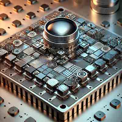
Micro-Optical Device mounted on a silicon wafer, featuring intricate micro-scale optical components. The background shows a cleanroom environment, emphasizing the precision and complexity of the device.

Get Your Silicon Quote FAST! Or, Buy Online and Start Researching Today!
What Substrates Are Used to Fabricate MEMS Optical Switches?
MEMS (Micro-Electro-Mechanical Systems) optical switches are devices that control the path of optical signals using microscale mechanical components. The substrates used in their fabrication are selected based on mechanical properties, optical characteristics, and compatibility with microfabrication techniques. Common substrates for MEMS optical switches include:
-
Silicon (Si): The most widely used substrate in MEMS technology due to its excellent mechanical properties, well-understood microfabrication processes, and compatibility with electronic integration. Silicon is also beneficial for its thermal conductivity and is suitable for fabricating precise and reliable MEMS structures.
-
Silicon-on-Insulator (SOI): This substrate includes a thin silicon layer separated from the bulk silicon by a buried oxide layer, providing electrical isolation and reducing parasitic capacitance. SOI substrates are ideal for MEMS optical switches as they enhance performance and reliability.
-
Silicon Dioxide (SiO2): Often used as a dielectric layer or a cladding material for optical waveguides on silicon substrates. SiO2 (Thermal Oxide) provides excellent optical transparency and electrical insulation.
-
Quartz (Fused Silica): Known for its high optical transparency, low thermal expansion, and chemical resistance, quartz is used in high-precision optical components within MEMS optical switches, ensuring minimal optical loss.
-
Gallium Arsenide (GaAs): Offers high electron mobility and direct bandgap properties, making it suitable for integrating optoelectronic components with MEMS switches. GaAs is used in applications requiring efficient interaction with light, such as in photonic integrated circuits.
-
Indium Phosphide (InP): Similar to GaAs, InP is used for high-speed optoelectronic and integrated photonic applications due to its direct bandgap and high electron mobility. InP substrates are beneficial for switches operating in the infrared spectrum.
-
Lithium Niobate (LiNbO3): Extensively used for its strong electro-optic and nonlinear optical properties, LiNbO2 is employed in MEMS switches that require efficient light modulation and switching.
-
Sapphire (Al1O3): Valued for its excellent thermal and chemical stability, as well as its optical transparency, sapphire substrates are used in harsh environments and applications requiring high durability.
-
Glass: Various types of glass, such as borosilicate glass, are used for their optical clarity, chemical resistance, and thermal stability. Glass substrates are used in the fabrication of optical waveguides and other components within MEMS optical switches.
-
Polymers: Flexible and low-cost polymer substrates, such as Polydimethylsiloxane (PDMS) and Polyimide, are used for their ease of processing and ability to form complex microstructures. Polymers are used in applications where mechanical flexibility is required.
Each of these substrates offers specific advantages for the fabrication of MEMS optical switches, with the choice depending on the required optical performance, mechanical properties, thermal stability, and integration needs of the device.

