Wafers Used In Optical Microscopes
A PhD candidate requested a quote for the following.
I am currently working in a university research group and I have some substrates that I need to procure asap. Please provide me with the quotes for Silicon substrate 3" P(100) SSP prime 1-10 Ohm-cm quantity :25 and Quartz Substrate Slide, Microscope, 25 x 25mm quantity: 3
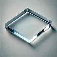
The slide for Optical microscope application is used non-single material, like glass wafers, and fused quartz wafers etc.
Question:
Will single quartz is work as a microscope slide?
Answer:
Seedless Single crystal quartz is typically quite smooth and hydrophilic, so it generally holds liquids well on a slide. Its smooth surface can facilitate even spreading of liquid samples, and its hydrophilic nature tends to keep the liquid in place without significant beading. However, depending on the thickness of the liquid layer and the nature of the liquid, you might observe some movement or spreading over time, especially if the surface has been modified or treated.
If you need the liquid to stay more stable or prevent evaporation, consider adding a coverslip to minimize the liquid movement and improve optical clarity.
Reference #93676 for specs and pricing.
Get Your FAST! Or, Buy Online and Start Researching Today!
Why Use Silicon Wafers With a Thick Thermal Oxide Layer Under an Optical Microscope?
Using silicon wafers with a thick thermal oxide layer under an optical microscope provides distinct advantages, especially in materials science and semiconductor applications. Here’s why a thick thermal oxide layer is beneficial:
Researcher:
I believe we wanted quite a thick oxide layer so that we could have significant contrast under optical microscope.
Reference #197158 for specs and pricing.
-
Enhanced Optical Contrast:
- A thick thermal oxide layer on silicon creates a high-contrast interface when viewed under an optical microscope. The oxide layer enables interference effects that increase the visibility of surface features, thin films, and defects, which would otherwise be challenging to see on bare silicon.
- The thickness of the oxide influences the degree of constructive and destructive interference, resulting in colors or contrast that highlight details on the wafer's surface.
-
Uniform and High-Quality Oxide Layer:
- Thermal oxide, grown by heating silicon in an oxygen or steam environment, provides a very uniform, high-quality layer with fewer impurities or surface roughness compared to other oxide deposition methods. This uniformity is crucial for consistent imaging across the wafer.
- Thermal oxidation forms a chemically stable, dense layer that adheres well to silicon, improving durability during microscopic analysis and reducing the likelihood of scratching or contamination affecting imaging quality.
-
Defined Oxide Thickness for Precise Contrast Control:
- The thickness of the thermal oxide layer can be precisely controlled during the oxidation process, allowing users to tailor the oxide thickness to optimize contrast at specific wavelengths. For example, oxide layers of hundreds of nanometers are commonly used to provide clear contrast under visible light.
- By choosing specific oxide thicknesses, researchers can enhance the visibility of different surface features based on their imaging needs. Thicker oxides tend to provide more uniform contrast without interference colors that can complicate imaging with thinner oxides.
-
Isolation and Electrical Properties:
- Thermal oxide is an effective electrical insulator, which is advantageous for certain electrical or electrochemical applications under an optical microscope. While this property is less relevant for purely optical imaging, it makes thermal oxide–coated wafers versatile for dual optical and electrical characterization setups.
-
Surface Chemistry Stability:
- The silicon dioxide layer is chemically inert and hydrophilic, making it stable in various environments. It does not easily react with environmental contaminants, which is beneficial for maintaining a clean, stable imaging surface under a microscope.
Overall, a thick thermal oxide layer on silicon wafers is an excellent choice for applications requiring enhanced contrast, uniformity, stability, and precise control over optical properties during microscopic analysis. These features make it ideal for inspecting thin films, microstructures, and surface defects in semiconductor and material science research.
What Is An Optical Microscope?
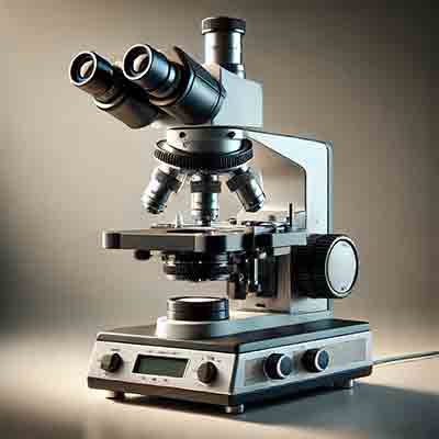
An optical microscope is a device that uses visible light and a series of lenses to magnify small objects, allowing them to be observed in detail by the human eye. It’s one of the most widely used types of microscopes and is commonly found in research labs, medical facilities, and educational institutions.
Key Components of an Optical Microscope
- Eyepiece (Ocular Lens): The lens you look through at the top of the microscope, usually with a magnification of 10x or 15x.
- Objective Lenses: Positioned on a rotating nosepiece, these lenses provide different levels of magnification (typically 4x, 10x, 40x, and 100x).
- Stage: The flat platform where you place your slides. It has clips to hold the slides in place and can often be moved with knobs for precise positioning.
- Light Source: An LED or halogen light
 illuminates the sample from below or above, depending on the microscope type.
- Focus Knobs: These knobs adjust the height of the stage (or the objective lenses) to bring the sample into sharp focus. The coarse focus provides general positioning, while the fine focus is used for detailed adjustments.
How It Works
- Illumination: The light source illuminates the sample.
- Magnification: The objective lens magnifies the sample image, which is then further magnified by the eyepiece lens.
- Observation: The final, magnified image is projected into the viewer’s eye or a camera, showing details not visible to the naked eye.
Types of Optical Microscopes
- Brightfield Microscope: The most common type, where light passes directly through the sample.
- Phase-Contrast Microscope: Enhances contrast in transparent specimens, ideal for observing living cells.
- Darkfield Microscope: Illuminates the sample from the side, creating a dark background and highlighting light-scattering features.
- Fluorescence Microscope: Uses fluorescence to illuminate and observe specific molecules within the sample.
Applications
Optical microscopes are used in various fields, including:
- Biology and Medicine: To observe cells, tissues, and microorganisms.
- Material Science: To study microstructures, thin films, and defects in materials.
- Education: In classrooms and labs to teach fundamental microscopy techniques.
Optical microscopes are prized for their simplicity, versatility, and relatively low cost compared to more advanced microscopes, like electron microscopes, making them essential tools for many scientific and medical applications.
What Substrates Are Can Be Used In Optical Microscopes?
In optical microscopy, substrates must be transparent (for transmitted light setups) or reflective (for reflected light setups) and should ideally provide a smooth, clean surface. Here are some commonly used substrates:
-
Glass
- Properties: Transparent, easy to clean, relatively inert, and inexpensive.

- Applications: Standard choice for most optical microscopy applications, ideal for biological specimens, slides, and coverslips.
- Fused Quartz
- Properties: Transparent to UV and visible light, high thermal and chemical stability, low birefringence.
- Applications: Suitable for high-temperature or chemical applications, as well as UV microscopy where glass may absorb too much light.
- Silicon (Polished)
- Properties: Reflective, opaque in visible light.
- Applications: Used for reflected light microscopy (e.g., metallurgical microscopy), semiconductor samples, microelectrodes, and nanofabrication studies. Polished silicon wafers can also be used for observing thin films on the surface.
- Sapphire (Aluminum Oxide)
- Properties: Transparent in the visible to infrared range, scratch-resistant, and thermally stable.
- Applications: Used in harsh environments or high-temperature studies, often chosen when durability and thermal resistance are critical.
- Calcium Fluoride (CaF2)
- Properties: Transparent from UV through the visible to IR, low birefringence.
- Applications: Ideal for UV microscopy or when studying samples across a broad spectrum, from UV to infrared.
- Plastic (e.g., Polystyrene or Polycarbonate)
- Properties: Transparent, flexible, inexpensive.
- Applications: Common for disposable slides or petri dishes, particularly in biological labs. However, plastic may scratch more easily and has limited chemical and thermal resistance.
- ITO-Coated Glass (Indium Tin Oxide)
- Properties: Transparent and conductive.
- Applications: Used when electrical conductivity is needed, such as in the study of electrochemical cells or transparent electrodes.
Question: I also need to do optical microscope on these glass. Any suggestions on type of glass and thickness?
Answer:
15-20 ohm/sq ITO coated glass
Size: 25x25x1.1mm
Glass: Japan LCD display grade, float glass
Good for optical microscope
Reference #201414 for more specs and pricing.
-
Aluminum or Gold-Coated Glass
- Properties: Reflective, conductive, non-transparent.
- Applications: Ideal for reflected light microscopy, especially with electron microscopy techniques, and for samples that require a conductive layer.
-
Silicon Dioxide on Silicon (SiO2/Si)
- Properties: Reflective with specific optical interference effects due to thin oxide layers.
- Applications: Used to enhance contrast in thin films, particularly in semiconductor and material science applications.
Each substrate offers unique benefits, and the choice depends on the sample properties, type of microscopy, and specific application needs.
What is Grain Boundary?
In the context of microscope slides or other materials, grain and grain boundaries refer to aspects of the microscopic structure of crystalline materials:
-
Grain:
- A grain is a region within a material where the atomic structure is uniformly aligned in a particular orientation.
- In polycrystalline materials (those made of many crystals or grains, like metals or ceramics), grains are the individual crystals that make up the bulk material.
- Each grain has a unique crystallographic orientation, which means the arrangement of atoms is slightly different from one grain to the next.
- The size, shape, and orientation of grains can affect the material's properties, such as strength, hardness, and optical clarity.
-
Grain Boundary:
- A grain boundary is the interface or boundary between two grains with different orientations.
- Grain boundaries are imperfections in the crystal structure because the atoms at these interfaces are not as neatly aligned as within the grains themselves.
- These boundaries can influence various material properties, including mechanical strength, electrical conductivity, and optical characteristics.
- Grain boundaries can act as barriers to dislocation movement, which can strengthen materials, but they can also be sites for corrosion or crack initiation.
In optical materials like glass microscope slides, the goal is usually to have a single-crystal structure (no grain boundaries) or a fully amorphous structure (like typical glass), where there are no grains or grain boundaries. This avoids scattering of light and maintains optical clarity, which is essential for microscopy.
How is an Optical Microscope used to determine the characterization of Graphene?
An optical microscope can be a surprisingly effective tool for characterizing graphene, particularly in determining layer thickness (number of layers) and uniformity of graphene sheets, when used in conjunction with certain substrate choices and techniques. Here’s how it works:
1. Visualizing Graphene Layer Thickness via Optical Contrast
- Graphene is typically transparent in the visible spectrum, but when placed on substrates like silicon wafers with a thermal oxide layer (commonly 90 nm or 300 nm), it becomes visible due to optical interference effects. The interaction of light with the thin oxide layer and the graphene sheet causes different contrasts that make graphene visible under an optical microscope.
- The contrast level changes with the thickness of graphene. Monolayer graphene, for instance, has a different contrast than bilayer or multilayer graphene, allowing researchers to estimate the number of layers based on optical contrast alone.
2. Identifying Graphene Thickness with Known Contrast Data
- Researchers have developed reference charts or software tools that correlate optical contrast values to the number of graphene layers, specifically on silicon dioxide substrates with known thicknesses.
- By comparing the observed contrast of the graphene sample under the microscope to these references, users can approximate the thickness (number of layers) of the graphene sheet. This technique is most reliable for few-layer graphene (1-5 layers).
3. Uniformity and Coverage Analysis
- An optical microscope allows for the visual inspection of uniformity across the substrate. Variations in contrast can indicate areas where graphene is thicker or thinner, as well as regions where there may be defects, wrinkles, or impurities.
- This type of inspection is especially useful in graphene production processes to quickly assess the quality of large-area films without requiring more advanced imaging techniques.
4. Detecting Defects and Contaminants
- Optical microscopy can reveal defects, such as cracks, tears, wrinkles, or folds in graphene. These defects are often visible due to light scattering or contrast differences.
- Contaminants on the graphene surface (like residues from transfer processes or environmental particles) may also appear under the microscope, allowing for a quick assessment of surface cleanliness.
5. Polarized Light Microscopy for Structural Information
- In some cases, using polarized light can help reveal additional structural information about graphene. Polarized light microscopy can enhance visibility of certain features, such as grain boundaries or orientation differences, especially in multilayer graphene.
6. Basic Raman Microscope Attachments
- Some optical microscopes are equipped with Raman spectroscopy attachments that can confirm the number of graphene layers and provide information about defects and doping levels. While not a purely optical microscopy technique, Raman spectroscopy is often combined with optical imaging to create a powerful characterization tool for graphene.
Summary
Optical microscopy, especially on silicon dioxide substrates with controlled thicknesses, allows researchers to:
- Estimate the number of graphene layers.
- Assess uniformity and coverage.
- Detect defects and contaminants.
While optical microscopy cannot provide the atomic-level detail of techniques like atomic force microscopy (AFM) or scanning electron microscopy (SEM), it is a rapid, accessible, and non-destructive method for basic characterization of graphene, especially when used as a preliminary check before more advanced analyses.

 illuminates the sample from below or above, depending on the microscope type.