
Need quote for Both side polished Silicon wafer (Intrinsic), the thickness 0.4 to 0.6mm, dia 4 to 6" (Qty. 50nos.) The wafers will be used with FTIR Spectrophotometer. Please confirm whether offered wafers will be IR transparent, no absorption in the IR.
Polished Silicon Wafer Inventory
A researcher requested a quote for the following:
Please reference #201657 for specs and pricing. Or buy online and save!
Polished silicon wafers offers single side and double side polished silicon wafers that are ready to use in your next project. We have over 20 years of experience producing high quality silicon wafers, so you can rest assured that you're getting the best product possible.
Get Your Quote FAST! Or, Buy Online and Start Researching Today!
Polished Silicon Wafers in Hard Plastic Wafer Carrier
Polished silicon substrates can be packed in several different ways. 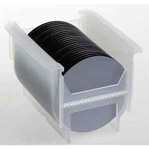 The most common is a hard plastic cassette that contains the wafer carrier below that supports the wafers for handling and shipping.
Below is a typical wafer with a polished surface that is reflective like a mirror. If these were DSP silicon, then both sides would be mirror like. If single side polished. The front side is considered the polished side. You can tell the back-side of the wafer as it will be opaque and not-reflective.
Mirror surface of the wafer.

Polished wafer in wafer carrier and cassette.
What Is Silicon Wafer Polishing?
The process of producing polished silicon wafers involves multiple steps, each of which is crucial to achieving  a uniform surface quality. The process starts by pouring molten silicon into a mold shaped like a silicon wave. This process eliminates the kerf, which is created by wire-sawing ingots into wafers. A second stage is used to produce double-sided (DSP) silicon. While this process is more complex and requires more technicians and equipment, it is the best method for achieving a smooth, flat surface.
The second step involves polishing the surface of the wafer by removing the top seven to fifteen micrometers of the wafer's surface. The process reduces the roughness of the surface to a level of about 10 nanometers Ra, which makes it ideally suited for IC fabrication. In addition, the amplitude of dopant striations is minimized to no more than 10 nm.
 Another process involves polishing the outer surface of the silicon wafer. The silicon wafer is mounted on an arm and then rotated on a ceramic turntable. The process polishes the silicon wafer to a high mirror finish using a high-pressure, high-frequency roller. The polishing step removes approximately 0.2 mm to 0.5mm of silicon from the surface. The process also reduces the surface roughness to 0.05 nanometers in an area of 1.6 cm 2.
Polished silicon substrates can be packed in a variety of ways. In a single-sided cassette, the wafer carrier supports the wafer. One side of the substrate is highly reflective, akin to a mirror, while the other side is opaque. In both cases, a hard plastic cassette is used to pack the silicon wafer. A typical polishing process reduces the surface roughness to 0.1 nm Ra, which is less than 0.05 micrometers per cm2.
A second polishing step is used to refine the surface of the silicon wafer. During this process, the silicon is roughened to a finish of 0.05 microns or higher. The surface roughness is measured using an optical interferometer. These measurements are important for the manufacture of electronic components. For example, the thickness of a chip is a small proportion of the width of a polished silicon wafer.
The first step in polishing is rough-surface polishing. This step is essential in achieving a flat surface. The surface of the wafer should be as smooth as possible. If the surface is not smooth, the polishing process cannot proceed. However, the finish polishing step is an important step for achieving a high-quality surface. After rough-finishing, the wafer is finished with a polishing solution that contains an alkaline etchant and an ammonia-stabilized colloidal silica slurry.
The final stage of polishing the silicon wafer is a crucial step for semiconductor production. This process is vital for ensuring that the silicon wafers are as smooth and as uniform as possible. A double-side polishing process is also useful for producing a more uniform surface in semiconductors. This process can be done on a smaller scale, and a single-sided polishing process can result in a better quality finished product.
The second stage of polishing is called finishing. The process involves a process that creates a mirror-like surface on a silicon wafer. A finished silicon wafer is the result of this process, which produces a surface with a smooth mirror-like appearance. The process also improves the quality of the silicon and improves its durability. Its low cost allows it to be a more affordable option than prime-wafers.
The surface roughness of silicon wafers can vary widely, depending on the processing methods employed. The most common technique involves using a single-sided polishing apparatus. This process begins by bonding a wax-coated wafer to a ceramic polishing block. Once the wax-coated slurry has been applied to the wafer, the arm of the rough polisher is then lowered until it comes in contact with a hard pad on a ceramic turntable. The ceramic turntable rotates while the polishing solutions are dispensed.
Single-sided polished silicon wafers are ideal for manufacturing devices with thin-film resistivity. The backside of the wafer should be as smooth as possible to avoid warping. A double-sided polishing process involves two processes. The first involves chemical mechanical polishing, while the second is physical. The first polishing method is a process called "surface cleaning" based on the atoms in the silicon. In this method, the silicon is etched with a chemical solution that removes surface metals and micro particles. The final product is a mirror-like finish.
How Do You Polish Silicon Wafers?
There are many textbooks and videos on how to polish wafers. But our engineers at UniversityWafer, Inc., are standing by to answer your questions quickly.
Save time. Ask your question today!
Polished silicon wafers with a smooth, mirror like surface are ubiquitous in the semiconductor industry for fabricating Integrated Circuits (ICs) surface. Polishing requires several steps and keeping the particle count to minimum is an absolute must to consider the wafers as pristine or prime grade. Chemical mechanical polishing (CMP) is the main method used by wafer fabs to polish substrates. CMP affects the surface of the wafer’s with chemicals by loosening the surface’s atomic bonding. The chemicals flow onto the wafer as it rotates on the polishing bed.
Researchers have been experimenting with other polishing methods to save on chemical costs and time. One potential method is to not polish at all. Instead a kerf-less method is used. Molten silicon is poured into a mold that is shaped like a silicon wafer of a certain size. The advantage of doing this saves on the kerf. Kerf is the dust that is the result of wire sawing an ingot into wafer form.
Double side (DSP) Silicon wafers and single side (SSP) polished silicon wafers are available. DSP wafers are much more complicated to fabricate as getting both sides of the wafer to be the exact as the other side is both art and science, and the equipment needed and technicians cost more.
Please forward any and all question for an immediate response.
Research Abstracts on Polishing Silicon Wafers
- Polishing pad's viscoelastic behaviour - silicon wafer flatness and chip yield
- Megasonic vibrations to assist in CMP of silicon wafers - New method to polish silicon wafers
- Setting up Abrasives to Polish Silicon - polishing pad research to create more efficient wafer polishing products from lapped to etch to polished wafers.
- Four Part Handbook on Polishing Silicon Wafers - Learn techniques to prepare silicon wafers for polishing detailed.
Polished Silicon Wafers Suitable for Hydrophilic Samples
Preparing hydrophilic samples can be difficult and time-consuming.
The traditional way to prepare a hydrophilic sample is to use a polished silicon wafer. This process can be difficult and time-consuming, especially if you are not familiar with the process.
At Polished Silicon Wafers, we offer high quality polished silicon wafers that are perfect for preparing hydrophilic samples. Our wafers are made from 100% virgin silicon, ensuring that they are of the highest quality possible. We also offer a variety of sizes and shapes to choose from, so you can find the perfect wafer for your needs.
We have polished silicon wafers that are suitable for hydrophilic samples (for standard HRSEM microscopy)
How Silicon Wafers Are Polished
The process of silicon polishing requires the preparation of a polished surface. A rough polishing process, at a temperature of 40 to 60deg C, removes approximately 7-30mm of the silicon's surface, resulting in a mirror-like finish. Afterward, the surface is left at room temperature to cure. This polishing procedure removes any imperfections from the surface. The result is a smooth, mirror-like surface for semiconductor devices.
Chemical mechanical polishing (CMP) is the most common method used to polish semiconductor wafers. CMP  is a multistep process in which the silicon is first polished using a coarse slurry, abrasive chemistry, and a high-nap polishing pad. In the first step of the process, the molten silicon is poured into a mold shaped like a silicon wafer. Afterward, the molten silicon is cleaned and then subjected to a process to remove any particle and chemical impurities. The next step is the finish polishing, which uses a finer abrasive chemistry and a softer polishing pad.
After the slurry has been removed, the silicon surface is cleaned by the polishing process. A multistep CMP polishing procedure is performed on the silicon wafer, consisting of a rough and a finish polishing step. This two-step CMP polishing procedure is illustrated in Fig. 1. In the rough polishing step, a coarse polishing slurry and aggressive etchant chemistry are used. In the final step, a high-nap polishing pad is used to remove any remaining particles.
A final step in the polishing process is to dry the polished surface. This step of the polishing process requires a certain amount of time. The minimum drying period depends on the drying environment and the type of silicon. The longer the drying time, the better the surface defect rate. After a rough polishing, the polished surface is then rinsed with deionized water to remove any residual chemicals. A warm gas or infrared lamp can also be used for active drying.
The CMP process of silicon wafers uses a slurry of chemical materials. A slurry is a liquid that is denser than water and is used to polish substrates. A slurry is an important step in the process of silicon polishing. It is an important step in the polishing process. It is essential for the smooth and flat surface of a semiconductor device. It is the first layer of a topographic surface. The subsequent layers are photoresists, which allow the image to be formed.
In this step, a slurry of nano-sized abrasive material is applied to the surface of the silicon wafer. The slurry is applied to the entire surface of the wafer. Typically, this process produces a mirror-like shine on the surface, but it can also damage the semiconductor wafer's structural integrity, which is what makes it such an attractive and useful product.
Another important step in the polishing process is planarization. The kerf-less process involves pouring molten silicon into a mold shaped like a silicon wafer. The kerf is the dust that results from wire sawing ingots into a wax-like surface. Double-sided (DSP) silicon abrasion requires more equipment and technicians to achieve the same result.
In this step, a thin layer of chemical slurry is applied to the surface of the silicon wafer. The slurry is composed of alumina-containing silane that forms a hydrophobic film on the surface. The chemical slurry is applied with a high-grade abrasive slurry. The slurry is an excellent way to prepare a silicon wafer for a new process.
The kerf-less polishing method is an alternative to conventional polishing. Instead of using a metal slurry, molten silicon is poured into a mold shaped like a silicon wafer. The kerf is a dust-free abrasive layer. The kerf-less polishing process can remove a thin layer of material. It is possible to create a smooth surface by coating a silicon wafer with an abrasive.
The process of silicon polishing uses a highly specialized method. The finished product, referred to as a silicon-based semiconductor, has a very smooth surface. The rough polishing process uses a high-grade, sodium-stabilized colloidal silica slurry. This slurry is then applied to the surface of the silicon wafer. This process is the best way to produce low-voltage MOSFET devices.
Why Are Silicon Wafers Polished?
The final step in semiconductor production, polishing of silicon wafers, is essential to make the surface of the silicon wafer smooth and uniform. The double-sided polishing process produces a smoother and more uniform surface than the single-sided process. The double-sided polishing process is more complex than the single-sided method and involves the use of more equipment and technicians. In addition, the double-sided polishing process produces a more uniform surface.
The process of polishing silicon wafers involves multiple steps, each crucial for achieving a uniform, smooth surface. In the first stage, molten silicon is poured into a mold shaped like a spherical wave. This eliminates the kerf, which is normally present in wire-sawing the ingot into a wafer. In the second stage, the layer of planarization is removed, creating a mirror-like surface.
The second step is to dry the surfactant solution. Using a drying period of twenty seconds reduces the amount of surface defects, whereas a shorter drying period decreases defect rate. The final step in polishing is to apply a polishing solution. The subsequent process liquid will be a rinse media. The surface will be opaque and non-reflective after being cleaned. This process is known as chemical mechanical polishing (CMP).
The final step is to remove any residual surfactant that is contaminating the silicon wafer's surface. The first step is called planarization, and involves the removal of 5-10 microns of silicon from the backside of the wafer. This process reduces micro-scale damage and stresses, and prevents warping. Once finished, the polishing procedure involves a cleaning and drying step that ensures that the silicon is squeaky-smooth.
The final step in silicon wafer fabrication is called chemical mechanical polishing. The polishing process requires the removal of any SOI films that are clinging to the surface of the silicon wafer. After this, the silicon wafer must be polished to produce an even surface. This step is also known as rheography. Its purpose is to create an even backside of the silicon wafer. There are a variety of other steps in the fabrication process of silicon wafers.
This process involves several steps. Each step is crucial to achieving a uniform surface. The first step consists of pouring molten silicon into a mold in the shape of a silicon wave. This eliminates kerf, which is caused by wire-sawing the ingots into a wafer. The second stage involves the removal of the second layer. Unlike the single-sided polishing, the double-sided polishing process requires more equipment and technicians.
A polishing process begins with the production of single-sided silicon wafers. These are ideal for thin-film resistivity, but are often too thin for thin-film applications. The back side of a silicon wafer should be smooth to prevent warping. The double-sided process involves a combination of chemical and physical polishing methods. The former involves the removal of micro-particles and surface metals.
Single-sided silicon wafers are the most common type of polished silicon wafer. These are ideal for thin-film resistivity, but the backside of the silicon is also critical. The double-sided process involves both physical and chemical polishing processes. The chemical mechanical polishing process removes the SOI films from the backside of the silicon. The physical polishing process eliminates the micro-particles and surface metals on the backside of the underlying silicon.
The process of polishing silicon wafers uses acidic solutions to smooth out the surface. The solution is neutralizing and controls the polishing reaction. The slurry is usually composed of an organic or inorganic acid or a mixture of acids. Aqueous acetic acid is representative of the acidic solution used in semiconductor-making. This solution is used to clean a silicon wafer. It is not only used in semiconductor manufacturing, but it also has many applications in the medical field.
The final step in the polishing process is to remove the etching stains on the silicon wafer. This is done by applying an infrared light or a warm drying gas. In order to get a high-quality surface, the etched silicon must be highly polished. During this process, the wafer must be smooth. It is necessary to ensure that the polished silicon wafer is free of defects.
What Are 300mm Silicon Wafer Applications?
In response to a growing demand for more semiconductor devices, Intel is now activating its $300mm silicon  wafer development program. The larger wafers will provide more than twice as much silicon surface area and more printed die than current 200mm (8-inch) wafers. It is estimated that this will reduce the cost of high-volume chip fabrication by as much as 30%. What are the benefits of 300mm wafers?
First, a larger wafer diameter will reduce manufacturing costs. The smaller the diameter, the lower the cost per die. For this reason, the industry has been experimenting with larger silicon wafers, such as those with 450mm diameters. While the newer sized wafers are difficult to form, they are proving to be highly beneficial in a number of industries. In fact, Intel has even been working on producing chips with a 450mm diameter.
Increasing the diameter of a silicon wafer can make it easier to create a chip. The larger the diameter, the more chips a company can produce on a single wafer. Moreover, the newer-sized wafers are more affordable. Consequently, this can reduce the cost per die by thirty or forty percent. In addition to the benefits of a larger diameter, a larger wafer allows for more die per wafer.
Currently, most 300mm silicon wafers are not made in-house. Rather, they are purchased from top suppliers around the world. But there are other benefits to a bigger diameter. This makes the production process more efficient. It also means that more chips can be produced on a single wafer. This makes 300mm wafers more expensive per die. The larger the diameter, the greater the cost-efficiency of a semiconductor.
A 300mm silicon wafer is more expensive than a 200mm one, but its increased size provides an edge over smaller ones. The cost per die of a microchip is lower than the one of a conventional silicon wafer. The larger the diameter, the more die a manufacturer can make. The higher the volume of a microchip, the more profit they can make. If a semiconductor manufacturer can produce more chips, it makes them more competitive.
Increasing the diameter of a silicon wafer increases the productivity of a manufacturer. The larger the wafer, the more chips it can produce. Using a 300mm silicon fab reduces the cost of a microchip by 30-40%. As a result, more chips can be made on a given wafer. Aside from that, the larger the diameter, the higher the productivity of a manufacturer.
A 300mm silicon fab will have a larger diameter than 200mm. Its size will increase throughput and lower the cost of semiconductor manufacturing. Despite the increased cost, the technology will improve efficiency for many industries. It will also help reduce the size of wafers and save money. It will also increase the number of applications for a 450mm fab. This will make it possible to make a broader variety of products and reduce the cost of a traditional wafer.
A 300mm fab will require a large amount of investment to develop the technology. For instance, the D1C technology development fab will include a 120,000 square foot clean room. The new fab is expected to cost $1.2 billion over the next few years. With a larger diameter, a 300mm lithography fabricated semiconductor fab will also increase its throughput. The 450 m lithography process will be the key for achieving higher speeds in these fields.
In addition to the benefits of a 300mm lithography fab, the 300mm fabs can be made up of up to 450mm-diameter wafers. Increasing the diameter of the fab will decrease the cost per die by up to 30%. A larger lithography fab will be able to make more chips in a shorter period of time. In addition to reducing the costs of fabrication, a higher-diameter lithography a larger lithography fabricated silicon fab will be more flexible.
Although 300mm silicon lithography enables higher-density, low-density silicon wafers are still relatively costly and do not perform well in electronics. To be an effective semiconductor, a silicon wafer must have a mirror-like surface. A perfectly polished 300mm silicon lithography ring is ideal. The material is suited for mass-scale manufacturing. A thin film is the perfect solution for many different electronic devices.
What Substrates are Used for Ellipsometry and Profilometry
Scientists have used the following Polished Wafers Item #783 - 100mm P/B (100) 1-10 ohm-cm SSP 500um Prime Grade for their Gas Barrier Thin Film Research.
What is Ellipsometry?
Ellipsometry is a scientific technique used to determine the surface optical constants of materials. The measurements are taken using a spectroscopic ellipsometer and are usually made on a thin film of polymer. These measurements can be made to an accuracy of a few angstroms.
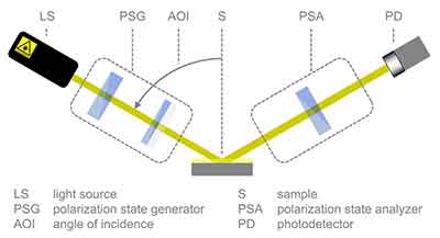
This type of measurement has its limitations, however. It has a low accuracy and must be done in conjunction with a thin film. It measures two parameters, Ps (Psi) and D (Delta). The two parameters, when measured with an ellipsometer, are used to calculate the sample's thickness and index of refraction. It can also be used to numerically invert a thin film interference equation.
One advantage of this technique is that it does not require a dark room. Moreover, the measurements are unaffected by polarized light. This makes ellipsometry superior to reflectivity measurements when analyzing anisotropic materials. A basic understanding of ellipsometry will allow you to use it effectively. If you are wondering: "What is Ellipsometry?", this article will give you an overview.
Modern ellipsometers use a range of radiation sources and detectors. Their spectral ranges range from the ultraviolet to the terahertz.
What is Profilometry?
Profilometry is a surface-contact measurement technique that is used to measure the surface topography of an object. This technique was originally used to measure the thickness of films. Today, the technology is used for a variety of applications, including the study of materials, such as metals and polymers.

Its basic components include a sample stage and a surface detection method. The detection method takes measurements of irregularities on a surface and enables it to create 3-D models of the surface topography. Some systems even have the capability to move the sample stage and detector. This gives the user the flexibility to measure different aspects of the surface's topography without disrupting it.
The most common use of a profilometer is to measure the roughness of a road. Generally, the instrument is connected to a moving test system, such as a standard car or specialized dolly. In both cases, it is a non-contact measurement method. The information gathered from profilometry is used to determine how to repair roads, and determine information that will affect the tire and drive system. This way, cars will be able to perform at their highest potential in varying road conditions.
In terms of the type of profilometers available, there are two main types. One uses a diamond tip stylus to measure surface textures. A computer then models the surface as the stylus moves across it. This method is much more accurate than non-contact systems, but it has its limitations. One major disadvantage is that the device is limited to samples, and a surface must fit under the reading needle.
Video: What is a Profilometer?