
"I would need a p-type wafer with both a 10 nm oxide layer and a deposited polysilicon layer (>250 nm) to avoid the hazardous CVD polysilicon deposition process."
Polysilicon Wafers and Thin Film Solutions
UniversityWafer supplies polysilicon wafers, deposited polysilicon films, and custom silicon wafer structures for semiconductor research, MEMS fabrication, integrated circuits, sensors, and photovoltaic applications.
Available configurations include:
- Polysilicon deposited on silicon wafers
- Polysilicon on SiO₂
- Thermal oxide / polysilicon film stacks
- P-type silicon substrates
- N-type silicon substrates
- Custom film thicknesses and dopant concentrations
- Single-side and double-side polished wafers
Request a Custom Polysilicon Wafer Quote
Need a custom polysilicon wafer? Tell us your substrate material, wafer diameter, orientation, oxide thickness, polysilicon thickness, dopant type, resistivity, polish, and quantity. We can provide standard inventory or custom-manufactured wafer structures for research and production.
Get Your Polysilicon Quote FAST! Or, Buy Online and Start Researching Today!
Customer Example: Polysilicon Gate Stack
A researcher developing an integrated circuit requested a thermal oxide and polysilicon gate stack to avoid performing in-house CVD deposition.
UniversityWafer supplied a custom 2-inch single-side polished p-type silicon wafer with a 10 nm thermal oxide layer and a deposited polysilicon film exceeding 250 nm.
Reference #264057 available for specifications and pricing.
Why Researchers Choose Polysilicon
Polysilicon remains one of the most important semiconductor materials because it combines excellent thermal stability with controllable electrical conductivity. Depending on the dopant concentration, polysilicon can function as a conductive electrode, resistor, or structural layer in semiconductor devices.
Researchers commonly select polysilicon for:
- Integrated circuits (ICs)
- MOSFET gate electrodes
- MEMS fabrication
- Thin-film transistors (TFTs)
- Solar cell research
- Microelectronics prototyping
- Semiconductor process development
What Is Polysilicon?
Polysilicon, also known as polycrystalline silicon, is an ultra-high-purity form of silicon used as the primary raw material for manufacturing semiconductor devices and crystalline silicon solar cells. Unlike monocrystalline silicon, polysilicon consists of many small silicon crystals, or grains, separated by grain boundaries.
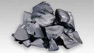
Electronic-grade polysilicon typically exceeds 99.9999999% purity (9N or higher) and is produced using processes such as the Siemens process before being converted into single-crystal boules or deposited as thin polysilicon films for integrated circuits and MEMS devices.
Because of its exceptional purity and controllable electrical properties, polysilicon plays a critical role in modern semiconductor manufacturing.
How Is Polysilicon Manufactured?
Most semiconductor-grade polysilicon begins with metallurgical-grade silicon derived from quartz. Through chemical purification and chemical vapor deposition (CVD), impurities are removed until electronic-grade purity is achieved.
The purified polysilicon may then be:
- Converted into single-crystal silicon using the Czochralski (CZ) or Float Zone (FZ) process
- Deposited as LPCVD polysilicon thin films for MEMS and integrated circuits
- Used directly for photovoltaic cell manufacturing
Researchers frequently combine polysilicon with SiO₂, silicon nitride, and other dielectric films when fabricating semiconductor devices.
Electronic-Grade vs. Solar-Grade Polysilicon
Although both electronic-grade and solar-grade polysilicon are produced from highly purified silicon, they are manufactured to different purity standards depending on the intended application.
Electronic-grade polysilicon typically exceeds 99.9999999% purity (9N or higher) and is used to manufacture semiconductor silicon wafers, integrated circuits, MEMS devices, power electronics, and other advanced microelectronic components where extremely low impurity concentrations are essential.
Solar-grade polysilicon generally has slightly lower purity requirements but is produced in much larger volumes for crystalline silicon photovoltaic cells. While both materials begin with purified silicon feedstock, electronic-grade polysilicon requires tighter control of metallic contaminants and dopant concentrations.
UniversityWafer supports researchers developing semiconductor devices, MEMS, sensors, and thin-film structures requiring high-purity polysilicon and custom silicon wafer configurations.
Custom Polysilicon Thin Film Structures
A PhD researcher requested a custom polysilicon/SiO₂/silicon wafer structure for semiconductor fabrication.
"I am looking for Polysilicon/SiO₂/Si wafers. How thick can the polysilicon layer be? Would it be possible to obtain 4-inch p-type silicon wafers with a polysilicon layer for our project?"
UniversityWafer supplied a 500 nm polysilicon / SiO₂ / silicon wafer on a 100 mm p-type boron-doped silicon substrate with a (100) orientation and one-side-polished surface.
Reference #320415 available for specifications and pricing.
What Is Polysilicon Used For?
Polysilicon is widely used throughout the semiconductor and photovoltaic industries because it combines excellent electrical performance, thermal stability, and compatibility with standard microfabrication processes.
Common applications include:
- Integrated circuits (ICs)
- MOSFET gate electrodes
- MEMS devices
- Thin-film transistors (TFTs)
- Photovoltaic (solar) cells
- Sensors
- Power semiconductor devices
- Research and prototype wafer fabrication
Depending on the application, polysilicon may be intentionally doped with boron, phosphorus, or arsenic to achieve specific electrical resistivity and conductivity requirements.
Polysilicon vs. Monocrystalline Silicon
Although both materials consist of silicon atoms, their crystal structures differ significantly.
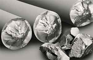
Monocrystalline silicon contains a continuous crystal lattice with virtually no grain boundaries, making it the preferred material for high-performance integrated circuits. Polysilicon consists of multiple crystal grains, making it easier and less expensive to manufacture while remaining suitable for many semiconductor and photovoltaic applications.
Both materials are essential to modern electronics, with polysilicon serving as the starting material for producing many single-crystal silicon wafers.
Polysilicon vs. Monocrystalline Silicon Comparison
| Property | Polysilicon | Monocrystalline Silicon |
|---|---|---|
| Crystal Structure | Multiple silicon crystal grains separated by grain boundaries | Single continuous crystal lattice |
| Purity | Typically 9N+ for electronic-grade material | Produced from electronic-grade polysilicon using CZ or Float Zone growth |
| Manufacturing Process | Chemical purification followed by CVD deposition (Siemens process) | Czochralski (CZ) or Float Zone (FZ) crystal growth |
| Relative Cost | Lower | Higher |
| Mechanical Structure | Polycrystalline with grain boundaries | Single crystal with virtually no grain boundaries |
| Primary Applications | Solar cells, LPCVD films, MEMS, transistor gates, research | Integrated circuits, power devices, MEMS, sensors, advanced semiconductor fabrication |
| Main Advantage | Lower manufacturing cost and versatile thin-film deposition | Highest electrical performance and crystal quality |
Key Properties of Polysilicon
Polysilicon combines excellent electrical, mechanical, and thermal properties with compatibility across standard semiconductor manufacturing processes. Its electrical conductivity can be precisely controlled through doping, making it suitable for transistor gates, resistors, sensors, and MEMS structures.
- Ultra-high purity available for semiconductor manufacturing
- Excellent thermal stability during high-temperature processing
- Electrical properties controlled through boron, phosphorus, or arsenic doping
- Compatible with LPCVD and other thin-film deposition processes
- Widely used in integrated circuits, MEMS, photovoltaic devices, and microelectronics research
Researchers frequently combine polysilicon with thermal oxide, silicon nitride, and other dielectric films to fabricate multilayer semiconductor structures.
What Is a Polysilicon Gate?
A polysilicon gate is the gate electrode used in many MOSFET devices. Deposited by LPCVD, polysilicon gates withstand high-temperature processing and allow precise control of transistor switching characteristics.
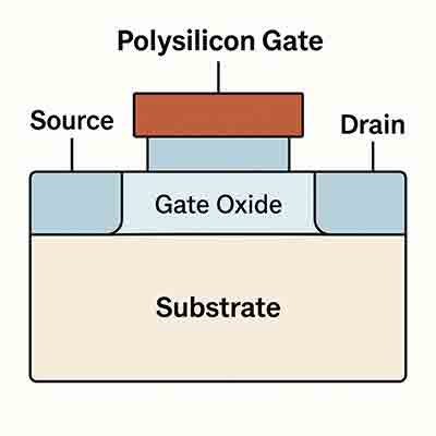
Although many advanced semiconductor technologies now use high-k metal gate (HKMG) structures, polysilicon gates remain important for MEMS devices, research, educational fabrication, and numerous semiconductor manufacturing processes.