Silicon Wafers for Spintronic Thin-Film Research
A professor of Electrical and Computer Engineering requested a quote for silicon substrates used to grow magnetic thin-film stacks for spintronic device research.
Research Application:
Our application is to grow magnetic thin-film stacks for spintronic nanostructures. The silicon wafer serves only as the substrate, so electrical conductivity through the wafer is not required.
We need a smooth, electrically insulated surface with 50-150 nm of SiO2 to support magnetic film deposition. Previously we evaluated both test-grade silicon wafers with 100 nm wet thermal oxide and prime-grade silicon wafers with 100 nm dry thermal oxide for this application.
Reference #273859 is available for specifications and pricing.
UniversityWafer supplies silicon wafers with thermal oxide for spintronics, magnetic tunnel junctions (MTJs), magnetic thin-film deposition, and other advanced semiconductor research. Custom oxide thicknesses, wafer diameters, crystal orientations, dopants, and polish options are available.
Get Your Spintronics Wafer Quote FAST! Or, Buy Online and Start Researching Today!
What is Spintronics?
 Spintronics, also known as spin electronics, is an advanced field of semiconductor research that uses the electron’s spin and magnetic moment, in addition to its electrical charge, to store, transfer, and process information.
Unlike traditional electronics, which rely mainly on moving electrical charge through a circuit, spintronic devices use spin states such as “up” and “down” as an additional way to represent information. This makes spintronics important for research in non-volatile memory, magnetic sensors, quantum devices, low-power electronics, and next-generation data storage.
Why Spintronics is Important
Spintronic materials and devices are studied because they may help improve speed, energy efficiency, and data retention compared with conventional electronic devices. Applications include MRAM magnetic random-access memory, magnetic tunnel junctions, spin valves, spin filters, spin transistors, and quantum computing structures.
Substrates Used for Spintronics
The substrate is important because it supports the magnetic and non-magnetic thin-film layers used in spintronic devices. Researchers often need smooth, insulating, and thermally stable surfaces for growing magnetic thin-film stacks, tunnel barriers, and nanoscale device structures.
Common substrates used for spintronics include:
- Silicon (Si): Used for magnetic thin-film stacks, semiconductor compatibility, and SiO2 insulated surfaces.
- Silicon with SiO2: Useful when researchers need an insulating oxide layer between the silicon wafer and magnetic films.
- Gallium Arsenide (GaAs): Used for high-mobility semiconductor spin transport and advanced device research.
- Magnesium Oxide (MgO): Often used in magnetic tunnel junctions and MRAM research because of its insulating properties.
- Sapphire (Al2O3): Provides a stable, high-temperature substrate for thin-film deposition and epitaxial growth.
- Indium Phosphide (InP): Used in specialized spintronic and optoelectronic research applications.
- Graphene: Studied for two-dimensional spin transport, high carrier mobility, and advanced nanoscale devices.
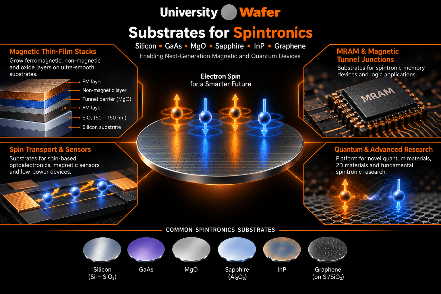
Silicon Wafers for Magnetic Thin-Film Stacks
Many spintronics researchers use silicon wafers with thermal oxide to grow magnetic thin-film stacks. A SiO2 layer can provide electrical insulation, surface smoothness, and separation between the silicon substrate and the magnetic materials deposited on top.
For spintronic nanostructures, common specifications include wafer diameter, oxide thickness, surface polish, dopant type, resistivity, orientation, and total thickness variation. Silicon wafers with 50 nm to 150 nm SiO2 are often requested for research involving magnetic layers and insulating surfaces.
UniversityWafer, Inc. supplies silicon, SiO2 coated silicon, GaAs, MgO, sapphire, InP, graphene, and other substrates for spintronics research and magnetic thin-film development.
Related Spintronics Resources
