Crystalline Silicon Wafers for Advanced Semiconductor Research
Crystalline silicon (c-Si) wafers provide a highly controlled
substrate platform for semiconductor device fabrication, thin-film research,
microelectronics, photonics, MEMS, and experimental device structures.
Researchers can specify crystal orientation, conductivity type, dopant,
resistivity, thickness, surface finish, and deposited films according to
their fabrication requirements.
UniversityWafer supplies
crystalline silicon substrates
as well as wafers with thermal oxide, amorphous silicon, epitaxial silicon,
and other deposited layers for specialized research.
Low-Temperature BEOL-Compatible Schottky Diode Research
One research application involves developing
Schottky-contact diodes using low-temperature deposited silicon.
A Ph.D. researcher requested a silicon substrate stack containing doped
amorphous silicon for investigating device fabrication at temperatures
below approximately 400°C.
“We need Si wafers with a layer of n-type doped amorphous silicon on top,
with a target doping concentration in the range of approximately
1018–1019 cm-3.
We are planning to fabricate low-temperature BEOL-compatible Schottky-contact
diodes using doped amorphous silicon. Previous work demonstrated the concept
with phosphorus-doped crystalline silicon and polycrystalline silicon
deposited at approximately 600°C. We now plan to investigate whether the
device can be fabricated using amorphous silicon deposited below 400°C
for improved BEOL compatibility.”
Requested substrate stack, from bottom to top:
-
100 mm (4-inch) silicon wafer
P-type, (100) orientation, approximately 1–20 Ω·cm resistivity,
single-side polished, test grade.
-
Thermal silicon dioxide (SiO2)
Approximately 1000 Å (100 nm) thermal oxide on both sides.
-
N-type amorphous silicon (a-Si)
Approximately 1000–2000 Å (100–200 nm) thick with target donor
concentrations around 1018 and 1019 cm-3.
Reference #273070 for specifications and pricing.
Why Low-Temperature Processing Matters for BEOL
Back-end-of-line (BEOL) processing occurs after many of the
temperature-sensitive device structures and interconnect layers have already
been fabricated. As a result, additional processing steps may need to remain
within a restricted thermal budget.
Depositing semiconductor films at lower temperatures can therefore be valuable
when researchers want to integrate additional devices without exposing existing
structures to the higher temperatures normally associated with some crystalline
or polycrystalline silicon processes.
Amorphous silicon (a-Si)
is particularly interesting for this type of research because it can be
deposited as a thin film at substantially lower temperatures than conventional
high-temperature crystalline-silicon processing.
Crystalline Silicon vs. Amorphous Silicon
Although both materials consist primarily of silicon, their atomic structures
are fundamentally different.
Crystalline silicon (c-Si) has long-range atomic order and,
under ambient conditions, adopts the diamond-cubic crystal structure.
Its controlled crystallographic structure makes it the standard substrate
material for many semiconductor and microfabrication processes.
Amorphous silicon (a-Si) lacks long-range crystalline order
and is generally deposited as a thin film. Its electrical and optical
properties depend strongly on deposition conditions, hydrogen content,
defects, and doping.
Polycrystalline silicon (poly-Si)
represents another form of silicon. It contains many crystalline grains
separated by grain boundaries and is widely used in semiconductor structures,
electrodes, gates, MEMS, and thin-film research.
Schottky Contacts on Silicon
A Schottky contact is formed at an appropriate
metal-semiconductor interface. Unlike a conventional p-n junction, its
electrical behavior depends strongly on the properties of the metal-semiconductor
interface, including the semiconductor doping, interface states, processing
history, and contact material.
Researchers can investigate Schottky structures using crystalline silicon,
polycrystalline silicon, or deposited amorphous silicon depending on the
device architecture and process-temperature requirements.
Controlled substrate resistivity and semiconductor doping are particularly
important because they influence carrier transport, depletion behavior,
contact resistance, and device characteristics.
Thermal Oxide as an Electrical Isolation Layer
The requested BEOL research stack includes approximately
100 nm of thermal silicon dioxide (SiO2).
Thermal oxide is commonly used as a high-quality insulating and dielectric
layer on crystalline silicon.
Depending on device design, SiO2 can provide electrical isolation,
surface passivation, masking, or a defined interface for subsequent thin-film
processing.
Explore
thermal oxide coated silicon wafers
for research requiring controlled SiO2 thicknesses on silicon
substrates.
Crystalline Silicon on Sapphire (SOS)
Crystalline silicon can also be integrated with insulating substrates.
Silicon-on-sapphire (SOS) consists of a crystalline silicon
layer grown on a sapphire (Al2O3) substrate.
SOS combines the useful electronic and nanofabrication properties of
crystalline silicon with the electrical insulation and optical properties
of sapphire. Depending on layer thickness and device design, this platform
can be useful for photonics, metasurfaces, RF devices, sensors,
microelectronics, and optical research.
Learn more about
silicon-on-sapphire wafers
.
Silicon-on-Sapphire for Metasurface Holograms
Researchers have used thin crystalline silicon layers on sapphire to fabricate
dielectric metasurfaces and holographic optical structures.
Patterning the high-index silicon layer into subwavelength structures allows
researchers to manipulate properties of transmitted or reflected light,
depending on the metasurface design.
One example of an SOS substrate supplied for this type of research included:
- Wafer diameter: 100 mm (4 inch)
- Substrate: Double-side-polished sapphire
- Sapphire thickness: 460 ± 20 µm
- Silicon layer: Epitaxial crystalline silicon
- Silicon orientation: <100>
- Silicon thickness: approximately 230 nm ±10%
- Resistivity: >100 Ω·cm
Other silicon-layer thicknesses may be available depending on research
requirements. Contact UniversityWafer for current specifications and
availability.
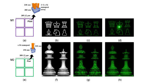
Example Application: Fabricated Metasurface Holograms
Applications of Crystalline Silicon Substrates
The combination of mature processing technology, controllable electrical
properties, high-quality surfaces, and well-characterized crystal structure
makes c-Si useful across a wide range of research applications, including:
- CMOS and semiconductor device research
- Schottky diodes and metal-semiconductor contacts
- Low-temperature BEOL device integration
- MEMS and microsensors
- Microfabrication and nanofabrication
- Metasurfaces and optical devices
- Silicon photonics
- Thin-film deposition research
- Solar cells and photovoltaic research
- Materials characterization
Selecting a Crystalline Silicon Wafer
The correct substrate depends on the fabrication process and final device.
Important specifications may include wafer diameter, thickness,
crystal orientation, conductivity type, dopant, resistivity, surface finish,
TTV, bow, warp, and deposited film requirements.
UniversityWafer supplies
crystalline silicon wafers
and custom thin-film substrate configurations for semiconductor,
microfabrication, photonics, MEMS, and materials-science research.
Get Your Crystalline Silicon Wafer Quote FAST!
Or,
Buy Wafers Online
and Start Researching Today!
Crystalline Silicon (c-Si) for Solar Cells and Semiconductor Research
Crystalline silicon (c-Si) is one of the most important
semiconductor materials used in modern electronics and photovoltaic technology.
Its well-ordered crystal structure provides predictable electrical, optical,
mechanical, and thermal properties that make it suitable for
solar cells, integrated circuits, MEMS, sensors, and semiconductor research.
In photovoltaic applications, crystalline silicon serves as the semiconductor
absorber in most conventional silicon solar cells. Researchers can control its
electrical properties through doping, surface processing, passivation, and the
formation of semiconductor junctions and contacts.
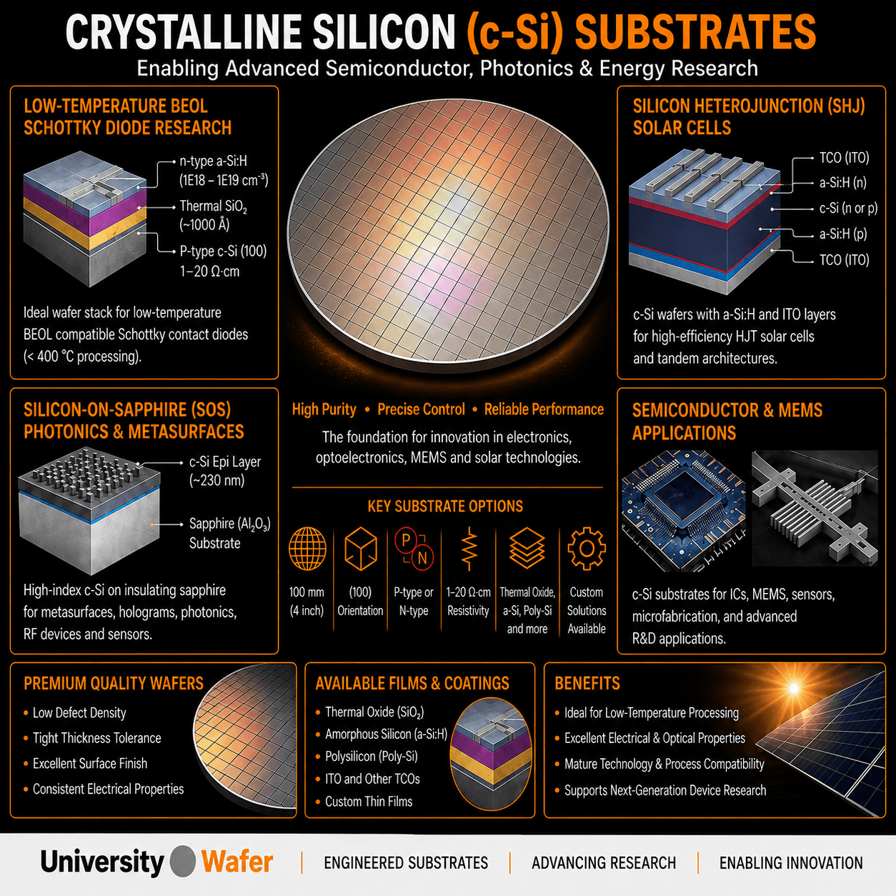
What Is Crystalline Silicon (c-Si)?
Crystalline silicon is solid silicon in which atoms are arranged in a
long-range ordered crystal lattice. At ambient conditions, silicon adopts the
diamond-cubic crystal structure, in which each silicon atom
is covalently bonded to four neighboring silicon atoms.
This ordered structure distinguishes crystalline silicon from
amorphous silicon (a-Si), which lacks long-range crystalline
order. Crystalline silicon can be produced as a single crystal or as a
polycrystalline material containing many individual crystal grains.
Learn more about
monocrystalline silicon
and its use as a semiconductor substrate.
Monocrystalline vs. Polycrystalline Silicon
Monocrystalline silicon consists of a continuous single-crystal
lattice across the material. Semiconductor-grade single-crystal silicon is
commonly grown using the Czochralski (CZ) or
Float-Zone (FZ) process.
Polycrystalline or multicrystalline silicon, by contrast,
contains multiple crystalline grains separated by grain boundaries. These
boundaries can influence carrier transport and recombination, making the
microstructure an important consideration in photovoltaic and electronic
applications.
For research requiring carefully controlled crystal orientation, resistivity,
doping, surface quality, and defect density,
single-crystal silicon wafers
provide a highly controlled substrate platform.
Crystalline Silicon vs. Amorphous Silicon
Crystalline and amorphous silicon are both used in photovoltaic technology,
but their atomic structures and electronic properties are substantially different.
Crystalline silicon has long-range atomic order and an
indirect band gap of approximately 1.12 eV at room temperature.
It is widely used for conventional wafer-based photovoltaic cells.
Amorphous silicon lacks long-range crystalline order.
Hydrogenated amorphous silicon (a-Si:H) is commonly deposited as a thin film
and can be used in thin-film photovoltaics as well as in passivation and
heterojunction structures.
These materials should not be confused with nanocrystalline or
microcrystalline silicon. Nanocrystalline silicon contains very small
crystalline silicon regions and therefore is not simply another name for
amorphous silicon.
Why Is Crystalline Silicon Used in Solar Cells?
Crystalline silicon combines several properties that make it well suited to
photovoltaic devices. Silicon is abundant, its semiconductor behavior is
extensively understood, and mature wafer-processing technologies allow
researchers and manufacturers to precisely control doping, junction formation,
surface texture, passivation, and electrical contacts.
When photons with sufficient energy are absorbed in the semiconductor,
they can generate electron-hole pairs. A properly designed photovoltaic
junction separates these photogenerated carriers, allowing electrical power
to be extracted through external contacts.
Solar-cell performance depends on much more than wafer size. Important factors
include material quality, minority-carrier lifetime, surface
recombination, optical losses, resistive losses, doping, passivation,
contact design, and device architecture.
P-Type and N-Type c-Si Wafers
Crystalline silicon wafers can be produced as either
p-type or n-type material by introducing controlled
concentrations of electrically active dopants.
P-type silicon
is commonly produced using acceptor dopants such as boron, while n-type silicon
is commonly produced using donor dopants such as phosphorus.
The appropriate conductivity type and resistivity depend on the intended
solar-cell architecture, fabrication process, and research objective.
Silicon Heterojunction Solar Cells
Silicon heterojunction (SHJ or HJT) solar cells combine a
crystalline silicon wafer with thin layers of hydrogenated amorphous silicon.
These thin films can provide excellent surface passivation while helping form
carrier-selective junctions.
Transparent conductive oxide layers, such as
indium tin oxide (ITO)
,
may also be incorporated to provide optical transparency and lateral electrical
conduction.
This combination of c-Si, a-Si:H, and transparent conductive
materials is widely studied for high-performance photovoltaic devices
and advanced tandem solar-cell architectures.
Crystalline Silicon in Tandem Solar Cells
Crystalline silicon can also serve as the bottom-cell absorber in
tandem photovoltaic devices. In these architectures,
a higher-band-gap top cell absorbs higher-energy photons while the silicon
bottom cell converts a portion of the longer-wavelength light transmitted
through the top device.
Perovskite/silicon tandems are an important research example. By combining
absorbers with complementary spectral response, tandem architectures can
potentially achieve conversion efficiencies beyond those obtainable from a
conventional single-junction silicon solar cell.
Silicon Wafer Orientation for Solar-Cell Research
Silicon wafers are available with crystallographic orientations such as
(100), (110), and (111). Orientation affects surface atomic
arrangement, oxidation, etching behavior, mechanical properties, and some
fabrication processes.
Si(100) is widely used in semiconductor processing and
silicon solar-cell research. Other orientations can be useful for specialized
experiments, particularly where anisotropic etching, surface structure,
cleavage, or crystallographic effects are being investigated.
Learn more about
silicon wafer orientation
when selecting substrates for a specific process.
Surface Texture and Light Management
Efficient solar cells are designed to minimize optical losses. Surface
texturing can reduce reflection and increase the effective optical path of
incoming light within the silicon absorber.
Crystallographic orientation is important because common anisotropic wet
etchants remove different silicon crystal planes at different rates.
On appropriately oriented wafers, this behavior can be used to create
microscopic surface structures for optical and microfabrication research.
Anti-reflection and passivation layers may also be deposited on the silicon
surface to reduce optical reflection and electronic recombination.
Six-Inch Silicon Wafers for Photovoltaic Research
150 mm (6-inch) silicon wafers
provide a useful research platform for photovoltaic device fabrication,
thin-film deposition, surface passivation, coating development, and
semiconductor processing.
Researchers can specify parameters such as wafer diameter, thickness,
crystal orientation, conductivity type, dopant, resistivity, surface finish,
and other material requirements according to their experimental process.
Applications of Crystalline Silicon Wafers
Although photovoltaics are an important application, crystalline silicon
substrates are used across a much broader range of research and manufacturing
technologies, including:
- Crystalline silicon solar cells
- Silicon heterojunction (HJT/SHJ) solar cells
- Perovskite-silicon tandem photovoltaics
- Integrated circuits and CMOS research
- MEMS sensors and actuators
- Microfabrication and nanofabrication
- Silicon photonics
- Thin-film deposition experiments
- Surface passivation research
- Semiconductor materials characterization
Selecting c-Si Wafers for Research
Selecting a crystalline silicon substrate requires more than choosing wafer
diameter. Depending on the application, researchers may need to specify
crystal orientation, thickness, dopant, conductivity type,
resistivity, surface finish, TTV, bow, warp, and crystal growth method.
UniversityWafer supplies
crystalline silicon wafers
for photovoltaic research, semiconductor fabrication, MEMS,
microelectronics, photonics, and materials-science applications.
Related Crystalline Silicon Resources
Explore related silicon substrates, thin films, semiconductor materials, and
fabrication technologies for electronics, photonics, MEMS, and photovoltaic research.
-
Silicon Wafers
– Explore crystalline silicon substrates available with different
orientations, dopants, resistivities, thicknesses, and surface finishes.
-
Monocrystalline Silicon Wafers
– Learn about single-crystal silicon and its use in semiconductor,
photovoltaic, MEMS, and materials research.
-
Amorphous Silicon (a-Si)
– Compare amorphous silicon thin films with crystalline silicon for
low-temperature processing and device research.
-
Polycrystalline Silicon (Poly-Si)
– Explore poly-Si materials used in semiconductor devices, MEMS,
electrodes, gates, and thin-film research.
-
P-Type Silicon Wafers
– Learn about acceptor-doped crystalline silicon substrates and
their semiconductor and photovoltaic applications.
-
Thermal Oxide Silicon Wafers
– Explore SiO2-coated silicon substrates for dielectric
isolation, device fabrication, and thin-film research.
-
Silicon-on-Sapphire (SOS) Wafers
– Discover crystalline silicon layers on sapphire for photonics,
metasurfaces, sensors, RF devices, and optical research.
-
Silicon Epitaxy
– Learn about epitaxial crystalline silicon layers for advanced
semiconductor structures and device development.
-
6-Inch Silicon Wafers
– Explore 150 mm silicon substrates for semiconductor processing,
thin-film deposition, and photovoltaic research.
-
Silicon Wafers for Solar Cells
– Learn about silicon substrates used in photovoltaic and
advanced solar-cell research.
-
Semiconductor Band Gap
– Learn how semiconductor band structure and band-gap energy
influence electronic and optoelectronic devices.
-
Microfabrication
– Explore wafer-based fabrication processes for semiconductor,
MEMS, photonic, and microscale devices.
