Germanium To Demonstrate Hall Effect
A PhD candidate requested the following quote:
We need Germanium wafers as per specifications below. We need Gemanium wafers both N type & P Type. Wafers are used in experiment boards which enables demonstration of the hall effect.
We need both P type & N type.
Picture of required wafer is attached herewith for your reference.
Length - 10mm +/- 0.05mm
Width - 5mm +/- 0.05mm
Thickness - 1mm +0.05/-0mm
Resistivity – 4-7 Ohm cm
UniversityWafer, Inc. Answered:
If you need these just to demonstrate the Hall Effect measurements, then I suggest that you use Silicon rather than Germanium - it costs less and is more readily available in size and resistivities that you specified. I can easily get you p-type Silicon (4-7)Ohmcm or more commonly (5-10)Ohmcm. I can easily get you n-type Silicon (4-7) or more commonly (5-10) or (3-9)Ohmcm.
Undoped Germanium generally has n-type conductivity in the range (1-10) or (5-30) or Ro>50 Ohmcm. It is difficult dope it with sufficient precision to achieve resistivity n-type (4-7)Ohmcm or p-type (4-7). Commonly doped Germanium is n-type Ge:Sb (0.01-0.05)Ohmcm and p-type Ge:Ga (0.01-0.05)Ohmcm.
You are better off with lapped rather than polished wafers. (100) orientation is most common so we would offer that, with the sides in (011) direction. Wafer dimensions and tolerances are appropriate.
We would probably offer round wafers, 1mm thick, diced into 10×5mm rectangles. They would be packed adhering to dicing tape, sealed in single wafer containers.
Reference #222096 for specs and pricing.
Get Your Quote FAST! Or, Buy Online and Start Researching Today!
Germanium Uses
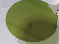 Our research clients use Ge Substrates for many purposes. Clients have used our 50.8mm Undoped Germanium wafers that are Double Side Polished as a dichroic mirror for Visible and Infrared light.
Visit our store to purchase directly or fill out the form for an immediate quote.
Dichroic mirrors and beam splitters are optical thin-film products that reflect, transmit, separate, or combine specific wavelengths (colors) and polarization components. Germanium substrates are often used for this purpose.
dichroic mirrors and beam splitters are used in:
- digital cameras
- mobile phones
- projectors
- other devices.
Related Semiconductor Material & Wafer Resources
What Applications Use Germanium Wafers?
Germanium substrates are semiconductor materials that are used in a variety of electronic devices, including transistors, solar cells, and infrared detectors. They are preferred for these applications due to their ability to conduct electricity and their optical properties, which make them useful for infrared applications. Germanium is also used as a substrate for growing other semiconductor materials, such as gallium arsenide, which is used in high-speed electronic devices.
How Can I Find the Cost of Semiconductor Materials Like Germanium?
The cost of semiconductor materials like germanium depends on the quantity you need to purchase. The price of a small amount is not crucial. The cost of a large quantity is, however, critical. A simple cost comparison shows that silicon is cheaper than germanium. The most important factor in determining the price of a semiconductor is the purity of the material. A high-purity material, such as silicon, will be more expensive than a low-purity one.
When comparing silicon vs. germanium, you will find that silicon is cheaper. This is due tothe fact that silicon has a higher melting point than its counterpart. However, you should also take into consideration the lower electrical conductivity of germanium. While this is a consideration, silicon is still more widely used in consumer electronics. For those that are concerned about the price of semiconductor materials, you can compare prices online.
The price of semiconductor materials is an essential element to the cost of electronic devices. As the manufacturing of semiconductors is constantly changing due to new technology, it's important to keep up with the latest prices and research in the industry. In addition, semiconductors are made from many different materials, so it's imperative to stay up-to-date with the latest developments. How can I find the cost of the most common semiconductor materials?
How can I find the cost of semiconductor materials?
Today, semiconductor manufacturing has undergone a great change in the way they are made. You can find the latest prices and research by reading industry news. Buying this type of material can be expensive, so you need to know the cos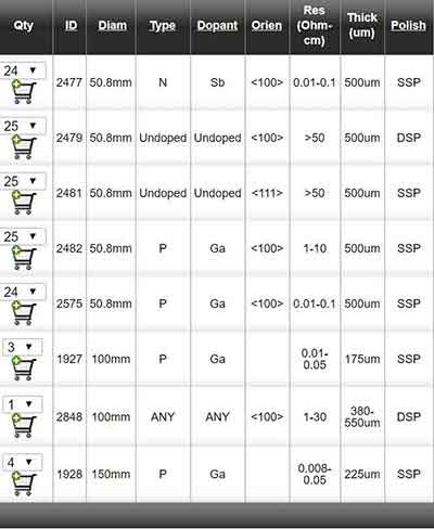 ts. Fortunately, it's easy to find the price of germanium in the market. So, if you're an electrical engineer, you'll need to know where to buy it and how much it costs.
 If you're wondering how to find the cost of semiconductor materials like germanium, you can check out the latest industry news. You can get the latest information about the prices of these materials in the news. You can also read industry-related articles about the current price of the material. These articles are helpful for the research and development of the industry. If you're in the industry of semiconductor manufacturing, you can use the latest material prices in your products.
You can find the cost of semiconductor materials by reading industry news. It's also a good idea to check the price of other materials. Listed below is a list of some of the most popular semiconductor materials. You can find the price of other types of semiconductor materials. Despite the recent price hikes, germanium remains a popular material to purchase. Aside from the competitive advantage, it's inexpensive and easy to obtain.
Various types of semiconductor materials have different properties. For example, silicon is more pure than germanium. It can be used to make computer chips. The disadvantage of using silicon is its low price. It's also a better choice if you need a high-purity semiconductor material. These materials can be used for other electrical purposes and will not have a high price tag. So, check the price before you buy.
In the last two years, silicon has become the preferred choice for manufacturing semiconductor devices. It is cheaper than germanium, and is more easily processed. It also has higher thermal and electrical resistance. Therefore, it is a better choice for consumer electronics. It is not easy to find the cost of semiconductor materials like germanium, but you can check its price on the internet. The best source to buy semiconductor materials is a reputable company that focuses on high quality and reliability.
While the cost of semiconductor materials is important for electronics, it is essential to remember that the price of semiconductor materials can fluctuate dramatically. The best place to buy semiconductor materials is online. If you are a retailer, the pricing of semiconductors is often listed on the website. If you want to purchase a specific type of silicon, you can compare the price against other products that are available. If the cost is higher than you'll pay for a more expensive product, you may want to consider buying less of it.
What Are Germanium Wafers Used For
Engineers at the University of Utah have developed a new method of cutting thin wafers with the chemical element germanium, and a patent has been filed for this. Bamberg compared the method of mass production to an egg-cutter, but the new way of cutting solar cell wafers, known as wire electrodischarge processing (WEDM), wastes less germanium and produces more of the wafers by cutting even the thinnest of them, with less waste and cracks. A new method that uses multiple parallel charged electric wires to cut gGermanium waves. [Sources: 5]
Although the new method makes germanium-based solar cells more efficient than silicon-based solar cells, Bamberg said, they could not be used as much as they used to be because they were too thin for use in a variety of applications such as solar panels, solar photovoltaics and solar thermal energy. [Sources: 5]
Moreover, the silicon-germanium market is too small for large players to work on the technology that could produce wafers and the devices. Instead, he said, it would be necessary to invest in developing its own technologies to gain large market shares. [Sources: 8]
There is growing interest in the use of silicon germanium in SiaGe alloys, which are used as materials for microelectronics and optoelectronic devices. There is increasing interest in identifying new technologies to increase semiconductor material production, such as the use of silicon germanium as a high-performance material for photovoltaics, and there is also increasing interest in using silicon and germanium for semiconductors in the automotive industry and for medical devices. [Sources: 0, 4, 8]
Silicon-germanium technology (SiGe technology) has been available for several years, but is only used in niche applications. The technology to combine germ and silicon materials to produce silicon-g germanium alloys has so far only been available for niche applications, and silicon and gGermanium technologies (SiGe technologies) are used in a range of applications, including photovoltaics and optoelectronic devices, as well as medical devices. [Sources: 8]
GaN - SiC substrates are mainly used for power semiconductors, automotive electronics and GaN / SiC substrate is mainly used in semiconductor and automotive electronics devices. GaAs materials, partially insulated gallium arsenide (gGermanium) and gGermanium - gSi, are mainly used in electronic devices, mainly in photovoltaics and optoelectronics, as well as in medical devices and medical applications. HF Front - End (PA) HF and HF - Frontend PA, Ga as Si is used, but Ga Since materials are mainly used in optical devices (e.g. in high-performance and low-energy optics). [Sources: 3]
If silicon is the most commonly used material, silicon wafers are called "wafers" because the crystal material is specified as silicon wafers - gGermanium - silicon (Si - wafers). If silicon is used, which is one of the three most common semiconductor materials, or silicon is indicated as Si but no crystal materials, this is called a "wafer." If silicon is a material most commonly used in electronic devices such as semiconductors and electronic systems, and no crystals of this material are specified, the silicon wafer refers to a cotton swab. [Sources: 3]
In this case, a germanium wafer can be embedded with silicon or a single crystalline wafer having an epitaxial layer of g germanium forming the outermost surface of it. The entire surface contains a layer of silicon, gGermanium and some other biomolecules, such as boron dioxide (BOD). The g germanium dissolves and the biomolescules remain on the surface that was originally uncoated. [Sources: 1, 6]
Germanium wafers are heated to the end and then the heat source is switched off until the alloy of the film is finished. Germanium wafers are heated in the presence of arsenic vapor diffusing from the heated polycrystalline g-germanium. The advantage is that the same heater that should be used to alloy the gold base layer with one side g Germania can be used to alloy the collector electrodes with the opposite side gGermania. This can be achieved by positioning the g Germanyia wafer in its usual form on a strip heater. [Sources: 2]
Place a clean g of germanium waffle in the oven to make it easier to keep it copper-free and bedridden, and then load it into an oven. [Sources: 2]
The wafers are also implanted with ions, etched and photolithographically patterned, which is not necessary for solar cells. In the first demonstration of their technique, the researchers used a one-atom-thick strip of graphene that they had sampled on a germanium wafer. Germanium - boron - co - doped substrate, but it was etched with a heavily doped substrate and a plasma - doped substrate with germ and borson, and a substrate dosed with both, in addition to a high dose of doped boron. [Sources: 7, 9, 10]
Germanium wafers were prepared by providing them with the outermost surface buffer layer, and the surface roughness of the polished germanium wafer was measured in relation to the effective value in the same way as in Example 1. As shown in Table 1, the polish was used for polishing, but the warp bow had the advantage of indicating that the germanium-doped silicon was hardly inclined to the wafer consisting of monocrystalline ingots. [Sources: 6, 10]
Sources:
[0]: https://patents.justia.com/patent/6833195
[1]: https://journals.plos.org/plosone/article?id=10.1371/journal.pone.0195062
[2]: http://www.google.com/patents/US3116184
[3]: https://www.utmel.com/blog/categories/semiconductor/analysis-of-semiconductor-wafers
[4]: http://www.google.si/patents/US6833195
[5]: https://www.reliableplant.com/Read/13425/slicing-solar-power-costs-with-new-wafer-cutting-method
[6]: https://patents.google.com/patent/EP3176810A1/en
[7]: https://phys.org/news/2016-09-chip-method-limited-wafer-space.html
[8]: https://www.prnewswire.com/news-releases/global-silicon-germanium-materials--devices-market-focus-on-material-type-source-substrate--epitaxial-wafer-device-type-wireless-radio-fot--end-user-telecommunication-consumer-electronics-automotive---analysis--fo-300648925.html
[10]: https://www.intechopen.com/books/advances-in-solid-state-circuit-technologies/germanium-doped-czochralski-silicon

 Our research clients use Ge Substrates for many purposes. Clients have used our 50.8mm Undoped Germanium wafers that are Double Side Polished as a dichroic mirror for Visible and Infrared light.
 If you're wondering how to find the cost of semiconductor materials like germanium, you can check out the latest industry news. You can get the latest information about the prices of these materials in the news. You can also read industry-related articles about the current price of the material. These articles are helpful for the research and development of the industry. If you're in the industry of semiconductor manufacturing, you can use the latest material prices in your products.