EpiWafers for Research
A teaching assistant from a large public university requested a quote for the following:
I need some epiwafers.
Diameter: 100 mm
Dtucture: 2 layers
Bottom layer: thickness 500 um n+-Si P concentration 1E19 cm-3
top layer: thickness 10 um p-Si B concentration 7e15 cm-3
please quote for quantity of 1 to 25 asap.
which method is the best way to realize this structure? I'm now considering epitaxial growth and ion implantation.
What's the price if we add a 1.5um Al contact layer at the bottom of the n-type layer.
The p type layer will be our top layer and we will build more layers on it, so this side need to be polished.
The n type layer will be our bottom layer.
Referece #210870 for specs and pricing. Or click here for the specs.
Get Your Quote FAST! Or, Buy Online and Start Researching Today!
Can Sapphire Wafers Be Used For Epitaxial Growth?
A university postdoc requested help with the following.
We are looking for supplier of epiready clean-room packed sapphire wafers for molecular beam epitaxy.
The maximal wafer size for our MBE apparatus is 1", normally we grow on 20x20x (0.3 ... 1.0) mm substrates.
At first, we would like to order several wafers in order to check their quality. Are the wafers really epiready ? How do they packed ? Can I use them for the epitaxial growth without any additional cleaning and chemical treatment ? If yes, could you please send me an official quote for:
- Sapphire, A-plane (11-20), +/- 0.1 deg, 1"x (0.3 - 0.8 mm), one-side polished, 10 pcs
- Sapphire, A-plane (11-20), +/- 0.1 deg, 20 mm x 20 mm x (0.3 - 0.8 mm), one-side polished, 10 pcs.
Reference #101799 for specs and pricing.
What is Epitaxial Growth?
It's all about layering one crystal on top of another, dude. Think materials science and semiconductor production - it's where this process shines the most. The cool part is how the new crystal takes its cue from the substrate beneath, copying its structure like a mirror image. Gives you a whole new level of respect for crystals, doesn't it? The term "epitaxial" comes from Greek roots meaning "arranged upon." In this process, the crystal lattice of the grown layer follows the pattern of the underlying substrate, ensuring that both have the same Ori. This matters a lot, you know, because it lets us make stuff with super precise and controlled features.
This approach is fundamentally instrumental in the manufacturing of a wide spectrum of semiconductor devices - we're talking integrated circuits, transistors and LEDs to name but a few! Epitaxial growth is achieved through methods such as Molecular Beam Epitaxy (MBE), Metal-Organic Chemical Vapor Deposition (MOCVD), and Liquid Phase Epitaxy (LPE). Every method boils down to one main action: carefully dropping atoms or molecules onto the base material. This allows that shiny new epitaxial layer to take shape, like a high-tech crystal growing kit!
The quality and characteristics of the epitaxial layer, such as its thickness, composition, and doping (adding impurities to change electrical properties), are crucial. The efficacy of semiconductors is intimately tied to their integral attributes. For example, in a light-emitting diode (LED), the epitaxial layer is responsible for the generation of light when electricity is applied.
Epitaxial growth? It's not just some fancy jargon for tech geeks. This process is at the heart of making stuff like advanced materials which are a big deal in photonics, quantum computing, and even solar cells - all that next-gen technology we're excited about! So, here's the deal. Epitaxial growth lets our brainy scientists and engineers create materials atom by atom - pretty cool, right? This isn't just some geek chic; it's pushing boundaries in tech and unlocking new opportunities across a wide range of fields. It’s as if we've got an all-access pass to the future!
What does Epitaxial Mean?
Epitaxial, you see, is all about growing a layer of crystal material on top of another crystal. It's like giving it a twin, but here's the cool part - this new layer follows the same pattern as its substrate. So it doesn't just sit there; it mirrors the underlying structure and creates an exact copy! This sync makes sure they're both headed the same way, key for making stuff with exact traits. Epitaxial growth, right? You'll find it a lot in the semiconductor world. It's all about crafting top-notch, tailored layers for stuff like integrated circuits and LEDs - super important tech we use every day. Techniques like Molecular Beam Epitaxy and Chemical Vapor Deposition (CVD) are employed for this purpose. Epitaxy is like the secret sauce in creating electronics, photonics, and high-tech materials. It's all about crafting stuff with particular atomic patterns and traits - kind of like a microscopic Lego set!
GaN/AlN/SiC Epitaxial Wafer
A professor of Chemical Physics requested the following quote for Synchrotron Radiation Research.
Please quote GaN/AIN/AI2O3 epitaxial wafer . 50mm in diameter, on-axis, n-type, GaN/AIN/SiC epitaxial wafer. Both 50mm in diameter on-axis, n-type. GaN thickness ~(0.5-0.8) um. AIN thickness ~0.1um. Please give pricing info for 1 or 5 wafers.
Reference #91327 for specs and pricing.
Epitaxial Definition
In the world of semiconductors, "epitaxial" means something specific. It's all about a thing called epitaxial growth, you see. So, imagine this. You've got a crystal substrate and you need to grow another crystalline layer right on top of it. That's what this technique is all about - kind of like building with blocks but at the molecular level! The key characteristic of this process is that the grown layer has the same crystallographic Ori as the substrate. In simpler terms, the atoms in the grown layer are arranged in the same pattern as the atoms in the substrate.
In the realm of semiconductor tech, epitaxial growth isn't just cool - it's vital. Why? Well, this process lets us build layers with incredible precision, not only in thickness but also composition. These features play a major role in creating diverse semiconductor devices, think transistors, LEDs, and integrated circuits. Why? Because you've got to have the electronic properties of your material under strict control for these babies to work right. Now, epitaxial growth - it's this slick method that lets us whip up top-tier materials with bespoke electronic attributes, pretty much a game-changer for anyone crafting cutting-edge tech or light-utilizing gizmos.
Gallium Nitride on Silicon Carbide Epitaxial Wafers
A ISO 14001 certified company requested a quote for the following:
I would quote, availability, wafer details on thk. res. etc. please. 1. GaN epitaxial wafers consist of GaN layer on 6H-SiC substrate. 50 mm diam on axis, n-type, GaN thickness ~0.5 um 2. GaN layer on sapphire, 50mm diameter on-axis, n-type, GaN thickness 0.5-10 um. 3. 2 " SiC. 6H. SSP, DSP 4. 2" Si. P type DSP.
Reference #90172 for specs and pricng.
Epitaxial Silicon Wafers
A nanomaterials researcher requested a quote for the following:
We are looking for <111> n/n+ epitaxial wafers with the epi thickness of 500 nm to 1 micron. Ideal resistivities are 0.1 and <0.01 ohm-cm for the epi and handle layers, but these are flexible. Time is also a major consideration. I would appreciate time and price quotes for wafers similar to these specs, particularly if you have them in stock.
Reference #103430 for specs and pricing.
Growing Epitaxial Layer on Silicon-on-Insulator Wafer
A PhD working in a semiconductor lab requese4d a quote for the following:
- I am looking for a thin film crystalline silicon layer of 2-4µm (p or n-type) on insulating substrate (could be an oxidized silicon wafer SOI). Do I have to buy the whole set of available wafers or can I buy 2 or 3 wafers only??
- I also would like to know if it is possible to grow an epitaxial layer on our samples (size 5x5 cm2) . It is a silicon layer on high temperature glass. Do you have any facility for epitaxial growth? I look forward to a promt answer.
Reference #94309 for specs and pricing.
Pn-Junction formed at the Wafer/Epitaxial Layer Interface
A PhD in Microstructure Physics requested a quote for the following:
We are looking for Si wafers (4" ideally) that can be either p or n-doped and have an epitaxial layer atop, so that a pn-junction is formed at the wafer/epi-layer interface. Can you offer anything? Thanks and best regards.
Reference #106430 for specs and pricing
Epitaxial Transistor
An epitaxial transistor is a type of transistor where one or more of its active layers, typically the base, collector, or emitter in a bipolar junction transistor (BJT), are formed using epitaxial growth. This growth technique allows for the deposition of a crystalline layer on a substrate with the same Ori as the substrate crystal.
In epitaxial transistors, the epitaxial layer provides several benefits:
-
Improved Performance: The quality and uniformity of the epitaxial layer can lead to better electrical  characteristics, such as higher electron mobility and lower defect density, enhancing the performance of the transistor.
-
Controlled Doping Profiles: Epitaxial growth allows for precise control over the doping concentration in different regions of the transistor. This is particularly important in BJTs, where the doping levels in the base, emitter, and collector regions significantly affect the device's performance.
-
Reduced Parasitic Capacitance: By carefully designing the epitaxial layers, it's possible to reduce unwanted parasitic capacitances, which can improve the speed of the transistor.
Materials used in the fabrication of epitaxial transistors include:
-
Silicon (Si): The most common material used for epitaxial transistors, especially in standard BJTs and MOSFETs (Metal-Oxide-Semiconductor Field-Effect Transistors). Silicon epitaxial layers are grown on silicon substrates.
-
Gallium Arsenide (GaAs)
and other III-V Compounds: These materials are used for high-speed and high-frequency applications. Epitaxial layers of GaAs and other similar compound semiconductors can be grown on substrates like GaAs or silicon.
-
Silicon-Germanium (SiGe): This is a popular material for high-speed bipolar transistors. SiGe can be grown epitaxially on silicon substrates, combining the advantages of germanium's high electron mobility with silicon's stability and maturity.
The choice of material depends on the application of the transistor. Silicon is generally preferred for digital circuits and standard analog applications due to its well-understood properties and mature processing technology. In contrast, materials like GaAs and SiGe are chosen for high-speed, high-frequency, and RF (radio frequency) applications.
Infrared Spectroscopic Measurements on Epitaxial Graphene
A physics professor requested a quote for the following:
We are performing infrared spectroscopic measurements on large area epitaxial graphene that will be deposited onto Si/SiO2 substrates. These measurements also require us to backgate the sample, so we need a compromise between low and high resistivity silicon in order to ensure that we can get light through the sample, while still being able to use a back gate. In addition the optical measurements require double side polishing. These specs are not common inventory for most companies, which makes them difficult to find in small quantities.
Reference #143652 for specs and pricing.
Multi-Layer Epitaxial Silicon Wafers
A PhD candidate requested a quote for the following:
Inquiry about a possible multi layer wafer. I wanted to procure some silicon wafers, and was wondering if you had any multi-layer wafers. I am looking for something with Bulk P-type low conductivity silicon (Layer 1), coated with a thin higher conductivity epitaxial silicon (Layer 2) and a silicon di-oxide layer (Layer 3).
I am looking for the following conductivity values and thicknesses of the layers: Layer # Conductivity (S/m) Thickness 1. Bulk Silicon (P-type) 5 0.5 mm 2. Epitaxial Silicon (P-type) 800 2 um 3. Silicon di-oxide 0 3.6 um Please let me know if it will be possible for us to get something of this sort. Also if it is not possible to get the exact conductivity values and thicknesses please let me know what values of these parameters we could get.
Reference #103963 for specs and pricing.
What is a Epitaxial Engineer?
A micro-optics researcher requested a quote for the following:
We are starting up an epitaxy fab and are looking to secure a supplier of both epi-ready sapphire wafers and GaN Sapphire wafers In particular we are looking to get availability and cost estimates 100 pcs and volume for Flat epiready sapphire substrates 2 4 6 wafer diameters Patterned sapphire substrates 2 4 6 GaN on flat sapphire substrates 5 um ntype Si doped 2 4 6 GaN on patterned sapphire substrates 5 um ntype Si doped 2 4 6 LED wafers blue andor green emitting 2 4 6 Thank you for your help in looking into any of the options above.
Reference #234639 for specs and pricing.
An epitaxial engineer is a professional who specializes in the field of epitaxy, a process used to grow crystalline layers on a substrate crystal in a manner that the layer mimics the crystal structure of the substrate. In the tech world, especially in areas like electronics and semiconductors, this job plays a big role. Why? Because it's all about making stuff that works really well - think transistors, lasers, integrated circuits. And to do that, they use something called epitaxial layers.
Key responsibilities and skills of an epitaxial engineer may include:
-
Process Development and Optimization: Developing and refining epitaxial growth processes to achieve desired material characteristics. This often involves working with techniques like Molecular Beam Epitaxy (MBE), Metal-Organic Chemical Vapor Deposition (MOCVD), or Liquid Phase Epitaxy (LPE).
-
Material Characterization: Assessing the quality of epitaxial layers using various characterization techniques such as X-ray diffraction, electron microscopy, and photoluminescence spectroscopy.
-
Problem-Solving: Troubleshooting issues related to epitaxial growth, such as defects, uniformity problems, or impurity control.
-
Collaboration: Working closely with other engineers and scientists, including process engineers, device designers, and quality control teams, to integrate the epitaxial layers into semiconductor devices effectively.
-
Venturing into the Uncharted:
Just as a movie adaptation of a bestseller sparks anticipation and judgment based on its alignment with our mental imagery, we're similarly embarking on an R&D journey—unearthing groundbreaking materials and novel methods—with emerging tech being our script, striving to shape visions of innovation while ensuring they remain rooted in reality. Engaging in R&D activities to explore new materials, epitaxial techniques, and applications in emerging technologies.
-
Having a good grasp of stuff like crystallography, semiconductor physics, and material science is key. Now think about it: how many times have you watched a movie that's based on a book? Often we judge the film by how well it sticks to our personal vision from reading the story. The same thing happens when we hear stories - our minds whip up visuals that are rich in detail, painting characters and places right before us. It's pretty fascinating! For anyone serious about mastering this, you've got to take a deep-dive into the complex realms of crystallography, semiconductor physics and material science - these areas aren't just important, they're absolutely pivotal.
This job's pretty hardcore, dealing with a lot of tech stuff. You're likely to need something like materials science or physics under your belt, maybe even chemical engineering. And we're talking grad-level knowledge here – no easy feat! Engineers specializing in epitaxy are the game-changers, pushing the boundaries of semiconductor tech. They're behind big breakthroughs in electronics and photonics, not to mention energy solutions.
LED Epitaxial Wafer
A Posdoc requested a quote for the following:
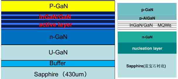
I like to know whether you sale GaN epitaxial LED wafers consist of p-GaN/MQW/n-GaN/u-GaN/sapphire or sale undoped or n-type GaN/sapphire only. If you sale the LED wafers, I like to buy a small quantity of blue or green LED wafers. Please let me know it via email. Thanks.
An LED epitaxial wafer is a critical component in the manufacturing of Light Emitting Diodes (LEDs). It is essentially a thin layer or layers of semiconductor material that have been epitaxially grown on a substrate wafer. This process involves depositing crystalline layers on the substrate in such a way that the crystal structure of the layers aligns with that of the substrate.
In the context of LEDs, these epitaxial layers are typically made from materials like Gallium Arsenide (GaAs), gallium nitride (GaN), or indium gallium nitride (InGaN), depending on the color of light the LED is intended to emit. These materials are chosen for their ability to efficiently emit light when an electric current is passed through them.
UniversityWafer, Inc. Quoted:
Pls see pics for detailed blue/green LED epitaxial wafer quotations.
Item 23 - 50.8mm GaN Epi Wafer C-plane Sapphire with 4.0um thick GaN Epi-Layer on SSP Sapphire
Item 24 - 50.8mm GaN Epi Wafer C-plane Sapphire with 6.0um thick GaN Epi-Layer on SSP Sapphire
Item 25 - 10mmmm GaN Epi Wafer C-plane Sapphire with 4.0um thick GaN Epi-Layer on SSP Sapphire
Item 26 - 10mmmm GaN Epi Wafer C-plane Sapphire with 6.0um thick GaN Epi-Layer on SSP Sapphire

The structure of an LED epitaxial wafer generally includes several layers, each with a specific function:
-
Substrate: Usually made of materials like sapphire, silicon, or silicon carbide, the substrate serves as the foundation for the epitaxial layers.
-
N-type Layer: This layer is doped with elements that provide excess electrons (negative charge carriers).
-
Active Layer: This is where light is generated. When electrons and holes (positive charge carriers) recombine in this layer, energy is released in the form of light.
-
P-type Layer: This layer contains holes created by doping with elements that accept electrons.
The precise engineering of these layers, including their composition and thickness, is crucial for determining the efficiency, color, and brightness of the LED. The epitaxial process allows for tight control over these parameters, enabling the production of LEDs with specific performance characteristics. The LED epitaxial wafer is then processed further to create individual LED chips.

 characteristics, such as higher electron mobility and lower defect density, enhancing the performance of the transistor.