Helping Process Integration Engineers
A process integration engineer requested help with the following sapphire quote.
I am curious to see your supply of Sapphire wafers with the following information : Sapphire C-plane <0001> +/- 1deg or 45 degree CCW C-axis (150 mm Sapphire) Projection onto R-plane +/- 1 degree DSP, Scratch/Dig 60/40 Diameter – 100 mm, 150 mm, 200 mm Thickness desired (range) – .7 mm to 2mm.
Can you let me know what options you have that may satisfy these specification, order qtys. and pricing if possible? I’m also curious about similar diameter and thickness possibilities you may have for a Si substrate, though am less aware of deviations in thickness from the SEMI standard.
Reerence #259392 for specs and pricing.
Highly Doped Silicon Used for Micro Nano Fabrication
A process integration engineer at a university micro nano fabrication dept. requested the following quote.
I am working in the Micro Nano Fabrication department.
We are looking for P++ wafers, 0.0008 ohmcm with 100-200nm LPCVD Si3N4 (possible with thin SiO2 layer below).
Do you have such wafers?
Reference #196764 for specs and quantitiy.
Get Your Quote FAST! Or, Buy Online and Start Researching Today!
Thermal Expansion Coefficient of Glass
A process integration engineer requested an answer.
I am writing to inquire a list of the coefficient of thermal expansion of your glass wafers. Please let me know if this is possible. Any kind of glass with a CTE between 2 and 6 ppm / C. Thanks!
Reference # 246369 for specs and pricing.
Epi-Structure Gallium Nitride (GaN) Substrates
A principal process integration engineer at a semiconductor company requested the following quote:
We would like to get quotation for bellow mentioned epi-structure. p+-GaN 100nm (Mg-1E19) i-GaN 2.5 um(Si-3E18) UID-GaN 1000 nm Sapphire (ooo1) Request you to give quotation on priority.
Here are the other details.
50mm (2”) – wafer.
Quantity : 25 pieces.
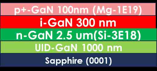
Other specs :
Roughness <0.5nm
FHWM < 300 arc sec
Doping concentration as mentioned above.
We need XRD and AFM for only one epi-structure (one piece) not for all 25 pieces.
Same way we need Hall for one epi-structure (n-GaN and p-GaN) not for all 25 pieces.
The important parameter I would like to know is Mobility of p-GaN layer. At least we are expecting approximate boundary or near by value if it is not precise. We are facing some issue in optimizing p-GaN ohmic contact. If you give reliable boundary or round value would be good enough to judge. Perhaps, our quotation included Hall data also, however considering your difficulty, try to give some valuable judgement on p-doping level.
Reference #268720 for specs and quantity.
Skills a Process Integration Engineer Needs
Process Integration Engineers require the following skills.
MEMS Process/Integration Engineer: Process Engineering in DRIE & Wafer Bonding Modules. FA and Yield Debugging. Participate in process transfer of new MEMS products and next generation electrostatic actuator process-architectures.
- Excellent working knowledge in Silicon Processing, or Vaccuum Science.
- Must have Hands on Experience in Cleanroom processing, in particular RIE or wafer level bonding.
- Experience in ElectroStatic Based MEMS Devices, in Theory, Design or Simulation is a plus.
- Good interpersonal and communication skills.
What Does a Process Integration Engineer Do?
A Process Integration Engineer in the semiconductor industry is responsible for integrating and optimizing various processes involved in semiconductor device fabrication. By closely monitoring each phase of manufacturing with an eagle eye on costs and quality standards; they guarantee our favorite items make it to shelves flawlessly. Here are some of their key responsibilities:
-
Process Development and Optimization 
- Develop and refine semiconductor fabrication processes.
- By refining how we do things now, we can get more done with less cost – it’s all about working smarter.
- Let's sit down with our process gurus – the engineers – and brainstorm on how to boost efficiency.
-
Cross-functional Collaboration :
- Work closely with design, manufacturing, and quality assurance teams.
- Coordinate with different departments to ensure process compatibility and integration.
- Serve as a liaison between R&D and manufacturing to ensure smooth technology transfer.
-
Troubleshooting and Problem-Solving :
- Spot the snags in how we mesh our procedures, then sort them out.
- Dive into the data, spot where things went sideways, and get straight to fixing them.
- Utilize root cause analysis and other problem-solving techniques.
-
Data Analysis and Reporting :
- Collect and analyze data from various stages of the manufacturing process.
- Picture this - we map out every step of our process, keep an eye on output fluctuations, and chase down any bugs messing with quality.
- Leverage handy statistical tools to keep an eye on how steady and capable our processes are.
-
Project Management :
- Let’s roll up our sleeves – either guide or join forces in refining how we tackle tasks.
- Juggle your project's schedule, money, and resources to make sure everything comes together just right.
- Ensure that projects meet specified goals and deadlines.
-
Process Documentation :
- Document process flows, procedures, and work instructions.
- Track every tweak you make to procedures and their fallout - it’s like piecing together a puzzle where each piece changes shape.
- Let's not just play by the book; let’s also ace our own high standards along the way.
-
Quality Assurance :
- Implement and maintain quality control procedures.
- Ensure that processes meet the required specifications and standards.
- Engage actively in audit sessions; it's how we ensure our work always meets gold-standard criteria.
-
Technology Advancement :
- Stay updated on the latest advancements in semiconductor processing technologies.
- Scout out the newest in technology – equipment or techniques – that promise big improvements.
- Pushing boundaries and integrating inventive strategies keeps us at the forefront – it’s how we outsmart competition every time.
A Process Integration Engineer is at the heart of creating top-notch semiconductor devices, masterfully blending different manufacturing steps into one smooth process.