
I used to purchase wafers from you in grad school and I purchased some sapphire substrates my first year here for a project. I was wondering if you knew much about the silicon wafer fabrication process. More specifically the kerf waste recovery methods silicon wafer manufactures implement. I have a project and we are trying to estimate the waste generated (around 40% for solar cell fabrication) but also account for waste recovery. There are a lot of waste recovery methods, but I don’t know what is commonly done in industry. Would you know or have any contracts who would know?
Silicon Wafer Fabrication and Kerf Waste Recovery
A Power Systems Researcher requested help with the following wafer fabrication question.
Reference #277031 for specs and pricing.
Wafer Fabrication Service
A wafer fabrication consultant requested the following:
I'm looking to find a company that can offer wafer fabrication as well as supplying the wafers. I've designed some optical SOI and SI3N4 ring resonator sensors and I need to get the wafers and the fabrication process done. Does your company provide the etching /fab process as well as supplying the wafers?
Si+sio2+si bonding process.
We perform mask production/etching/pattern production/deposition/polishing/CMP/dicing processes. We have entered into business agreements with our company/researchers at national and public research institutes industrialization support centers at universities around the world.
Please provide information about the required process, drawings, materials, etc.
Referenc #134946 for specs and pricing.
Get Your Quote FAST! Or, Buy Online and Start Researching Today!
UniversityWafer, Inc. along with our partners provide a vast number of fabrication processes to deposit metals, grow thermal oxide, thin and dice wafer etc.
Please let send us your wafer specifications along with quantity for an immediate quote.
Optical Ring Resonator Sensor Fabrication
A Postgrad (PhD) requested help with the following:
I'm a postgrad (Phd) and I'm looking to find a company that can 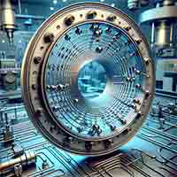 offer wafer fabrication as well as supplying the wafers. I've designed some optical SOI and SI3N4 ring resonator sensors and I need to get the wafers and the fabrication process done. Does your company provide the etching /fab process as well as supplying the wafers?
Reference #134946 for specs and pricing.
What is a Wafer Foundry?
A semiconductor wafer foundry is a facility that makes chips. The process is extremely complex, requiring hundreds of processes to make a chip. The final chip may have many layers and can take weeks to create. In Taiwan, the first "pure-play" semiconductor foundry was created, Microchip Technology, which also provides foundry services to other companies. The cost of establishing a new semiconductor plant can run into billions of dollars.
The process of building a semiconductor wafer starts with the formation of a silicon oxide film. Once the silicon oxide film has been formed, contact holes are drilled into it. Tungsten is then deposited in the contact holes and polished to remove excess tungsten. This is known as plug-tungsten filling. The next step is photo resist patterning, where a resist pattern is formed on the wafer. Copper metal is deposited in the trenches. This process is called a single damascene.
Another process is called Czochralski process. In this process, a solid silicon piece is placed in a bath of polycrystalline or molten silicon. As the liquid grows, it slowly pulls the silicon piece through rotation until it forms a cylindrical ingot. A finished wafer will look round. There are many different types of semiconductor foundries. Each of these types has their own unique capabilities and advantages.
The automotive industry has a high demand for semiconductor devices. For example, advanced driver assistance systems, autonomous self-driving vehicles, and power electronics for electric vehicles all require a significant number of electronic devices. While the automotive industry is a very competitive market, it is still a very lucrative sector for foundries. While many of these devices do not require cutting-edge processes, there are many vendors that are interested in entering this sector.
A semiconductor wafer foundry is a type of semiconductor foundry. The fabs are typically owned by the company that sells semiconductor chips. They manufacture these chips for third-party customers. A few examples of semiconductor chip manufacturing companies include Taiwan Semiconductor Manufacturing Company and GlobalFoundries. However, there are a number of different types of foundries. The process of creating the semiconductor chip is very complicated.
A semiconductor wafer is a predefined size. Its major sizes are 300mm and 200mm diameters. To create a semiconductor chip, you must first select the appropriate size for your project. For example, you can choose to produce a smaller or larger chip. A large-scale semiconductor wafer foundry can produce both small-scale and high-volume chips. Its size is the most important consideration for semiconductor manufacturing.
Today, there are many different types of semiconductor wafer foundries. These factories are usually located in Asia, with some of the largest ones being located in Taiwan. A semiconductor factory can be classified as a pure-play or non-pure-play wafer foundry. The former produces semiconductor ICs for other companies while a pure-play foundry mainly manufactures wafers for its own use.
There are several different types of semiconductor foundries. A semiconductor wafer foundry can be a pure-play or a non-pure-play one. A pure-play semiconductor foundry is a company that produces its own ICs. A non-pure-play semiconductor foundry produces wafers that are sold to other companies. A pure-play semiconductor manufacturer will typically provide a complete set of semiconductor products.
The first type is called a pure-play foundry. It is a semiconductor foundry that provides all of the necessary manufacturing services for a single product. These facilities are called a semiconductor foundry. They can produce chips using the same process as their customers. A pure-play semiconductor foundry can be either a non-pure-play or a pure-play company. The latter is a hybrid.
The process begins with a blank silicon wafer. Then, circuits are built in layers in a clean room. The first step is to cut a semiconductor ingot. A diamond saw is used to cut a semiconductor ingot into thin wafers. The size of the chip depends on the diameter of the semiconductor ingot. Then, a CMOS ingot is cut into a single, circular, or square piece.
The Silicon Wafer Fabrication Process
Silicon wafer fabrication involves transforming raw silicon into highly pure, defect-free wafers that serve as substrates for electronic and photonic devices. Here is an overview of the process:
1. Raw Material Preparation
- Silicon Source: Quartzite (SiO₂) is the primary source of silicon.
- Reduction: Silicon is extracted by heating quartzite with carbon in an electric arc furnace at ~2000°C to form metallurgical-grade silicon (MG-Si).
SiO2+C→Si+CO2
2. Purification
- Chemical Purification: Metallurgical-grade silicon is purified into electronic-grade silicon (EG-Si) or solar-grade silicon using the Siemens process:
- Silicon reacts with hydrogen chloride gas at ~300°C to form trichlorosilane (SiHCl₃).
- Trichlorosilane is purified through distillation.
- SiHCl3 is decomposed at ~1100°C to deposit pure silicon.
SiHCl3→Si+HCl
3. Crystal Growth (Ingot Formation)
- Czochralski (CZ) Method:
- A seed crystal is dipped into molten silicon and slowly pulled up while rotating.
- Produces large, cylindrical single-crystal silicon ingots.
- Float Zone (FZ) Method:
- A high-purity silicon rod is passed through a localized heating zone.
- Produces extremely pure single crystals, ideal for high-resistivity applications.
- Orientation: The crystal's orientation ([100], [111], etc.) is determined during this step.
4. Ingot Shaping
- Trimming: Ingot ends are removed, and the ingot is ground into a cylindrical shape.
- Flat/Notch Marking: Orientation flats or notches are added to indicate crystal orientation and doping type.
5. Wafer Slicing
- Wire Sawing: Thin diamond-coated wires slice the ingot into wafers of uniform thickness.
- Loss Minimization: Efforts are made to reduce kerf loss (wasted material during sawing).
6. Wafer Surface Preparation
- Edge Rounding: Wafer edges are rounded to reduce the risk of chipping and cracking.
- Lapping/Grinding: Removes surface damage from slicing.
- Chemical Etching: Further removes surface defects and damage.
7. Polishing
- Surface Planarization: Wafers are polished using a chemical-mechanical planarization (CMP) process to achieve a mirror-like finish.
- DSP vs. SSP:
- Double-side polished (DSP): Both sides are polished, typically for SOI or MEMS applications.
- Single-side polished (SSP): Only one side is polished, common for most applications.
8. Cleaning
- Ultrasonic and Chemical Cleaning: Removes contaminants, particles, and residues.
- RCA Cleaning:
- Removes organic contaminants.
- Oxidizes the surface and removes ionic impurities.
9. Inspection and Quality Control
- Dimensional Accuracy: Diameter, thickness, and flatness are measured.
- Surface Quality: Checked for defects like scratches, pits, or particles.
- Crystallographic Properties: Orientation, resistivity, and doping levels are verified.
10. Packaging
- Cleanroom Packaging: Wafers are placed in cassettes and sealed in clean, anti-static packaging to prevent contamination during transport.
This highly controlled process ensures the wafers meet the stringent requirements of semiconductor device manufacturing.
What is the Most Common Silicon Wafer Fabrication Process?
The most common silicon wafer fabrication process in the semiconductor industry is the Czochralski (CZ)  process. This process is widely used for producing single-crystal silicon wafers, which are the foundational material for most semiconductor devices, including integrated circuits and solar cells.
Here's a brief overview of the Czochralski process:
-
Silicon Melting: Pure silicon is melted in a quartz crucible at high temperatures (over 1400°C).
-
Seed Crystal Introduction: A small single-crystal silicon seed is dipped into the molten silicon. The seed crystal's crystallographic orientation determines the orientation of the grown crystal.
-
Crystal Growth: The seed is slowly pulled upwards and rotated simultaneously. As it is pulled, silicon from the melt attaches to the seed and crystallizes.
-
Diameter Control: By carefully controlling the temperature, the pull rate, and the rotation speed, the diameter of the crystal can be managed.
-
Crystal Shaping: The grown cylindrical single crystal, known as a boule, is then ground and shaped to have a perfect circular cross-section.
-
Wafer Slicing: The boule is sliced into thin wafers using a diamond saw or a wire saw.
-
Surface Finishing: The wafers are polished to achieve a smooth and defect-free surface, which is crucial for subsequent semiconductor device fabrication.
While the Czochralski process is the most common, there are other methods as well, such as the Float Zone (FZ) process, which is used in specific applications where higher purity and defect-free silicon is required. However, due to its scalability and cost-effectiveness, the CZ process remains the dominant method for silicon wafer fabrication in the industry.
What are Some Silicon Wafer Fabrication Techniques
The process of producing semiconductor chips includes thousands of steps and can take as long as three  months from conception to production. The first step involves cutting a thin piece of silicon wafer using a diamond saw. The silicon wafer is then cut into 'dies,' which can contain hundreds or thousands of chips. After cutting the wafer into the desired size, it must be annealed. This process is called sputtering.
After annealing, the silicon ingot is sliced into blocks with a diameter specified in the process. The peripheral is then ground to a specified diameter. The orientation of the crystal is indicated by a flat or notch on the surface of the wafer. Large and small diameter wafers are sliced using a laser-grinding process. Both of these processes are critical to the final Si material. Several processes are then used to polish the silicon crystals and make them as smooth as possible.
Deposition is the process of growing or coating materials onto the silicon wafer. Some of the deposition techniques used to achieve this include chemical vapor deposition, physical vapor deposition, electrochemical deposition, molecular beam epitaxy, and thermal oxidation. The next step in the process is to remove the materials. Chemical etching, atomic layer deposition, and mechanical planarization are all effective against specific types of elements.
The next step in silicon wafer fabrication is slicing. The slicing process creates a surface defect known as a saw mark. Lapping removes the saw marks and makes the wafer thinner. This also relieves the stress associated with slicing. After the lapping process, silicon wafers undergo an etching and cleaning process. The acetic and nitric acids are used to remove microscopic cracks and surface damage. The resulting material is then sliced and subsequently subjected to a series of manufacturing processes to ensure accuracy and smoothness.
The Czochralski method uses a small piece of solid silicon. It is placed in a polycrystalline silicon bath and slowly pulled into a cylindrical ingot. The finished wafer is a round disc. However, the Czochralski technique is more expensive than the other two. It is a relatively complex process. After sputtering, the crystal is ground. Once the surface has been cleaned, the silicon wafer is placed in the polishing bath.
The sputtering process involves the removal of rough spots and making the surface smoother. The sputtering process is an efficient and cost-effective way to polish silicon wafers. Depending on the size of the wafer, the final product may have a varying p-well or a single channel of the same type of hole. The final sputtering step is important because it makes it easier to see the shape of the in-plane structures that are used in IC production.
The Czochralski method begins by exposing a small piece of solid silicon to a bath of molten polycrystalline silicon. Once the silicon sputtering solution reaches the desired temperature, it is shaped into a cylindrical ingot. The sputtering process is an excellent way to make thin, round silicon wafers that are ideal for use in electronics. After the process is complete, the silicon wafer is polished to produce the finished product.
Once the silicon wafer is fully grown, it is sliced again. After slicing, the silicon wafers are examined under high intensity lights. This process is vital because it prevents the silicon from developing defects. After the lapping procedure, the silicon wafers are packaged and shipped in an airtight plastic bag to avoid contamination. There are several other steps in the fabrication process. The first step is slicing.
The next step in the process of silicon wafer fabrication involves adding dopants. These are elements from Groups 3 and 4 of the periodic table that affect the properties of the molten silicon. The range of dopants is extensive, but some common elements include Boron, Antimony, and Arsenic. A high concentration of dopants is essential for the production of semiconductors. The final step is the lithography stage.
The Czochralski method is the most popular of the silicon wafer fabrication techniques. The Czochralski method involves using a polycrystalline silicon ingot and adding dopants that give the desired electrical properties. A typical N-type ingot contains phosphorus and boron. Its high purity allows it to be used for a variety of applications, including semiconductor devices. The thickness of the silicon wafer is crucial for the semiconductors.
Silicon Wafer Fabrication Production Process
In this article, we will look closely at what makes silicon wafer production process different from other silicon manufacturing processes. [Video]
How Do You Fabricate Integrated Circuits?
The design of an integrated circuit requires a series of manufacturing steps, in which 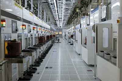 precise amounts of chemicals are injected into selected areas of a silicon wafer to form microscopic devices and compounds. A single silicone wafer goes through hundreds of process steps before the finished wafers are ready, leading to the production of ingots that are fed into electronic products. This gradually reduces the ASP of the ingot, which in turn lowers production costs. The lower ASP for silicon The reason for this is the pressure from the solar and PV cell industry. [Sources: 3, 4, 9, 11]
The huge capital investment of the G450C consortium participants has become sustainable, as the consortium also ensures the ability to generate a steady demand for newly produced silicon. However, it will take several years for new suppliers to meet the demand for the next generation of high-end electronics from new silicon wafers. [Sources: 1, 9]
This would help us to analyse the market for semiconductor wafer factories in the future. This would help us to analyze the silicon wafers, fabs, devices and the market for the next generation of high-end electronics and other semiconductors in our market. [Sources: 2]
The semiconductor wafer fab equipment market is divided into three major segments: silicon wafers, fab fab devices, devices and equipment. Apart from that, it is dominated by various types of devices such as semiconductors, chipsets, components and other materials. Monitoring the wafer production environment includes monitoring the temperature, humidity, temperature and humidity that the silicon wafer is exposed to, which can negatively affect its production yield. [Sources: 2, 14]
The pertinent observation is that the scope of functioning of silicon wafers is much higher than that of compound semiconductors. The above data analysis has taught us that in order to ensure the quality of the silicon produced in semiconductor wafer factories, it should not be used in the manufacture of electronic products. In the manufacture of top-class silicon wafers, manufacturers rely on wathers specialists such as Pure Wafer to help test top-class shafts and support the films to fully optimize the production process. [Sources: 3, 9, 11]
With continued investment in innovation, UniversityWafer, Inc. was founded to keep pace with the next generation of semiconductor technologies. We also offer special services, including the production of high quality silicon wafers for medical and electronic products. UniversityWafer, Inc. collaborates with some of the largest medical electronics manufacturers in the country and provides the highest quality silicon wafer manufacturing equipment and services. Through America's leading research and science universities, we provide the best education, training, and technical support to the medical industry. [Sources: 10, 11]
Our wafers are not the only place where silicon is used, and they are not even close to the largest consumer silicon. UniversityWafer, Inc. has been selected by some of the leading military contractors in the US Army, Navy, Air Force, Marine Corps, Army Corps of Engineers, Department of Defense and many other government agencies. The UniversityWafer, Inc. website is one of the few that provides access to a comprehensive list of equipment and services for the production of silicon wafers. Our two leading suppliers demonstrate our ability to produce flawless silicon wafers, controlling more than 90% of the world's medical electronics and medical device production capacity, as well as the vast majority of the world's medical devices. [Sources: 0, 6, 10, 12]
Many of China's domestic silicon suppliers supply wafers up to 150mm or smaller, but silicon wafer manufacturers are experiencing booming demand, resulting in tight supply and high prices for wafers. [Sources: 1, 5]
While China's silicon wafer suppliers continue to lag behind international peers in manufacturing capacity, the region's silicon production ecosystem is maturing and becoming more integrated. Due to the rapid growth of silicon production in China, according to a recent report by the Chinese Academy of Sciences, the country's central and local governments have enabled the financing of several silicon wafer production projects in recent years. [Sources: 1]
The Wafer Semiconductor Factory (FAB), built in India, is the first of its kind in the world and an indication of what India can do in terms of silicon wafer production capacity and supply chain integration. The idea of setting up a wafer production facility for S-semiconductors [F AB] unit in India is a clear indication that India could do well as a major silicon manufacturing center in the Asia-Pacific region. [Sources: 8]
The five largest wafer manufacturers, which generate more than 90 percent of the market revenue, are the first to do so. The advantage of working with larger diameters is more pronounced, as the basic material costs for compound semiconductors are lower. More recently, the ability to build these devices at a lower cost per square inch than traditional semiconductor wafers has led the industry to produce a wide range of high-performance, low-power devices. Cooperation is essential to ensure lower costs and better product quality for the consumer and commercial markets. [Sources: 1, 3, 7, 9]
Sources:
[0]: https://blog.lamresearch.com/silicon-wafers-and-more/
[1]: https://roboticsandautomationnews.com/2019/01/10/china-silicon-wafer-production-capacity-growth-fastest-in-the-world-says-semi/20480/
[2]: https://www.transparencymarketresearch.com/semiconductor-wafer-fab-equipment.html
[3]: https://www.businesswire.com/news/home/20191106005708/en/Global-Semiconductor-Silicon-Wafer-Market-Report-2019
[4]: https://www.computerhistory.org/revolution/digital-logic/12/288
[5]: https://semiengineering.com/mixed-outlook-for-silicon-wafer-biz/
[6]: https://www.universitywafer.com/top-things-you-should-know-about-silicon-wafer.html
[7]: https://patents.google.com/patent/US6312525B1/en
[8]: https://analyticsindiamag.com/india-semiconductor-chip-manufacturing/
[9]: https://www.semi.org/en/macroeconomics-450mm-wafers
[11]: https://www.globenewswire.com/news-release/2020/08/13/2078320/0/en/Pure-Wafer-s-Announces-wafersontheweb-com-Largest-Selection-of-Prime-and-Test-Grade-Silicon-Wafers-for-Semiconductor-Fabrication.html
[12]: https://www.tel.com/museum/magazine/material/150430_report04_03/02.html
[14]: https://www.thermofisher.com/ca/en/home/industrial/manufacturing-processing/manufacturing-processing-learning-center/electronics-information/semiconductor-analysis-imaging-metrology-information/chemical-analysis-semiconductor-fabs-process-wafer-environment.html
Do all solar cell manufactures recycle their Kerf or is it only some percentage of them?
Waste from the silicon cutting or polishing process is filtered through a filter, then the ground powder is  separated and reused for sandblasting and abrasive production. Depending on the size of the powder, it is separated into powders ranging in size from #100 to #3000. The manufacturer pays a fee to process the waste, and the processor receives a fee. After collection, a recycling company reprocesses the product and resells the product. Separation uses various methods such as /filter /centrifugation/sedimentation/chemical treatment/temperature heating...etc.